Eureka AIR delivers breakthrough ideas for toughest innovation challenges, trusted by R&D personnel around the world.

Method for driving liquid crystal display

a liquid crystal display and display technology, applied in the direction of instruments, static indicating devices, etc., can solve problems such as deteriorating display quality, and achieve the effect of reducing display brightness distortion

Inactive Publication Date: 2008-11-20
HIMAX DISPLAY INC
View PDF8 Cites 8 Cited by
  • Summary
  • Abstract
  • Description
  • Claims
  • Application Information

AI Technical Summary

Benefits of technology

The present invention provides a method for driving liquid crystal units and a liquid crystal display that can prevent the circuit from being influenced by a capacitive coupling effect, which can cause display brightness distortion and image sticking. The method includes a driving method for liquid crystal units with a first and second switch, a first and second storage capacitor, a first and second display-enable switch, and a pixel electrode. The method also includes a method for driving a liquid crystal display with a first and second write-able switch, a first and second storage capacitor, a first and second display-enable switch, a pixel electrode, and a data line. The invention aims to improve the display quality and user experience of liquid crystal displays.

Problems solved by technology

Moreover, as the accumulation of the residual charges on the pixel electrode causes an image sticking effect, this deteriorates the display quality.

Method used


Image

  • Method for driving liquid crystal display
  • Method for driving liquid crystal display
  • Method for driving liquid crystal display

Examples


first embodiment

The First Embodiment

[0025]FIG. 3 is a driving circuit diagram of a liquid crystal unit according to a first embodiment of the present invention. In this embodiment, switches are implemented by transistors, and each transistor has a gate, a drain, and a source. Referring to FIG. 3, the liquid crystal unit 300 includes a first switch S1, a first capacitor C1, a second switch S2, a pixel electrode M11, and a reset switch Srst. The gate of the first switch S1 is coupled to a scan line WA, and the source is coupled to a data line CH1, and the drain is coupled to a first end of the first capacitor C1. The second end of the first capacitor C1 is coupled to a ground end GND. The gate of the second switch S2 is coupled to a display signal line DA, the source is coupled to the first end of the first capacitor C1, and the drain is coupled to the pixel electrode M11. The gate of the reset switch Srst is coupled to the reset signal line RST, the source receives a reset voltage signal Vrst, and t...

second embodiment

The Second Embodiment

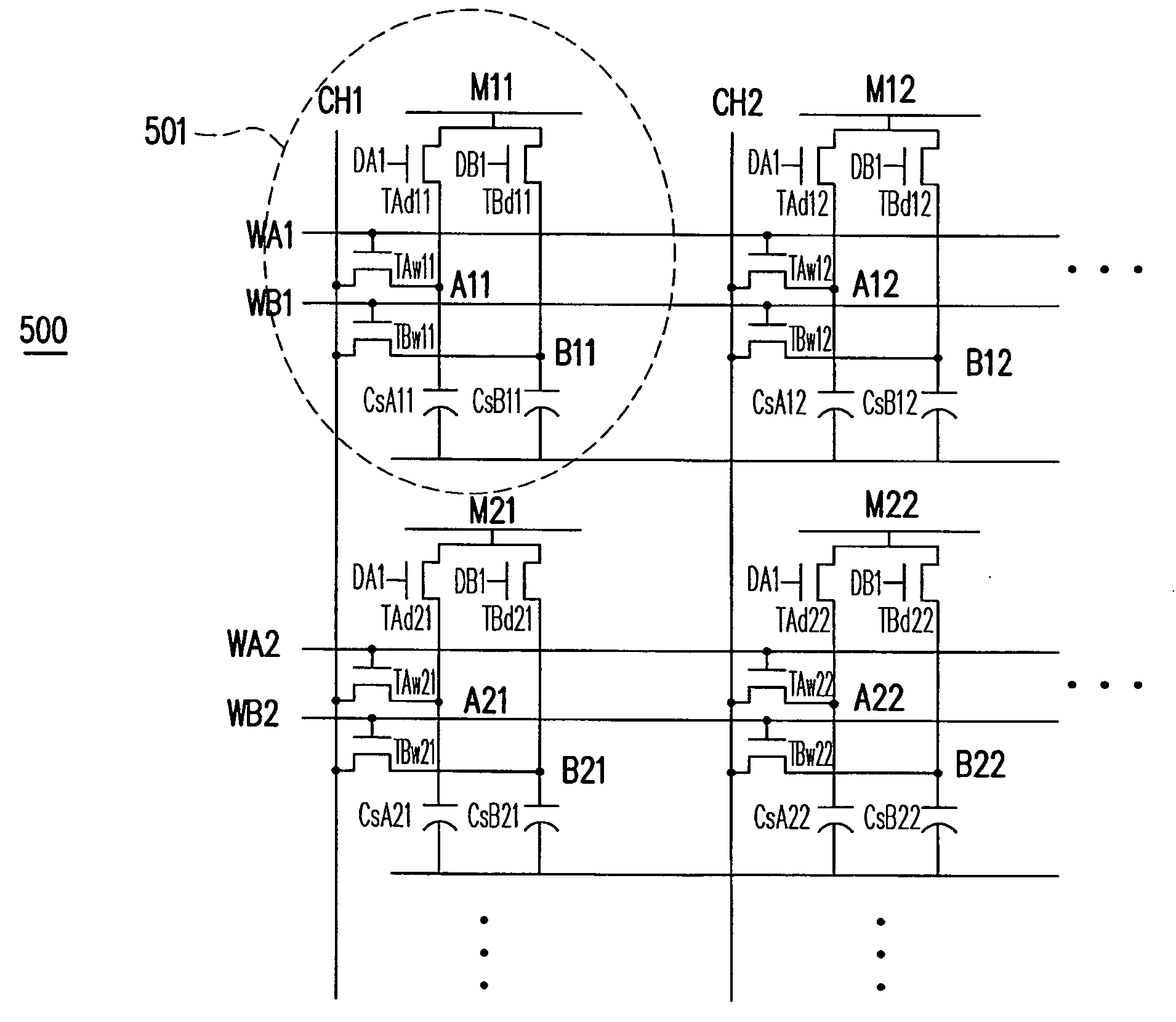
[0028]FIG. 5 is a driving circuit diagram of a liquid crystal display according to a second embodiment of the present invention. In this embodiment, switches are implemented by transistors, and each transistor has a gate, a drain, and a source. Referring to FIG. 5, the liquid crystal display 500 includes a plurality of liquid crystal units. For example, the liquid crystal unit 501 includes a first and a second write-enable switches TAw11 and TBw11, a first and a second storage capacitors CsA11 and CsB11, a first and a second display-enable switches TAd11 and TBd11, a pixel electrode M11, and a data line CH1. The liquid crystal display 500 displays a first frame and a second frame in a first and a second frame time respectively, and each of the first and the second frame time further includes a liquid crystal response time, a light display time, and a reset time.

[0029]The gate of the first write-enable switch TAw11 is coupled to a first scan line WA1, the source ...

third embodiment

The Third Embodiment

[0034]FIG. 7 is a driving circuit diagram of a liquid crystal display according to a third embodiment of the present invention. In this embodiment, switches are implemented by transistors, and each transistor has a gate, a drain, and a source. Referring to FIG. 7, the liquid crystal display 700 includes a plurality of liquid crystal units. For example, the liquid crystal unit 701 includes a first and a second write-enable switches TAw11 and TBw11, a first and a second storage capacitors CsA11 and CsB11, a first and a second display-enable switches TAd11 and TBd11, a pixel electrode M11, a data line CH1, and a reset switch Tr11. The liquid crystal display 700 in a first and a second frame time displays a first and a second frames, and each of the first and the second frame time further includes a liquid crystal response time, a light display time, and a reset time.

[0035]The gate of the first write-enable switch TAw11 is coupled to a first scan line WA1, the source...


PUM


Abstract

A method for driving a liquid crystal display is provided. The method includes: turning on a display-enable switch to pass through time of liquid crystal response and light display of a first frame until a reset time appeared. At the same time, turn on a second write-enable switch to pre-deliver a pixel signal corresponding to a second frame to a second storage capacitor. During reset time of the first frame time, turn on a reset switch and provide a reset voltage signal to a pixel electrode while the first and the second display-enable switches and the first and the second write-enable switches are turned off, in which the reset voltage signal has a first voltage level during a first period, and a second voltage level in a second period. Therefore, the method can increase brightness of the display, and decrease image sticking effect thereof.

Description

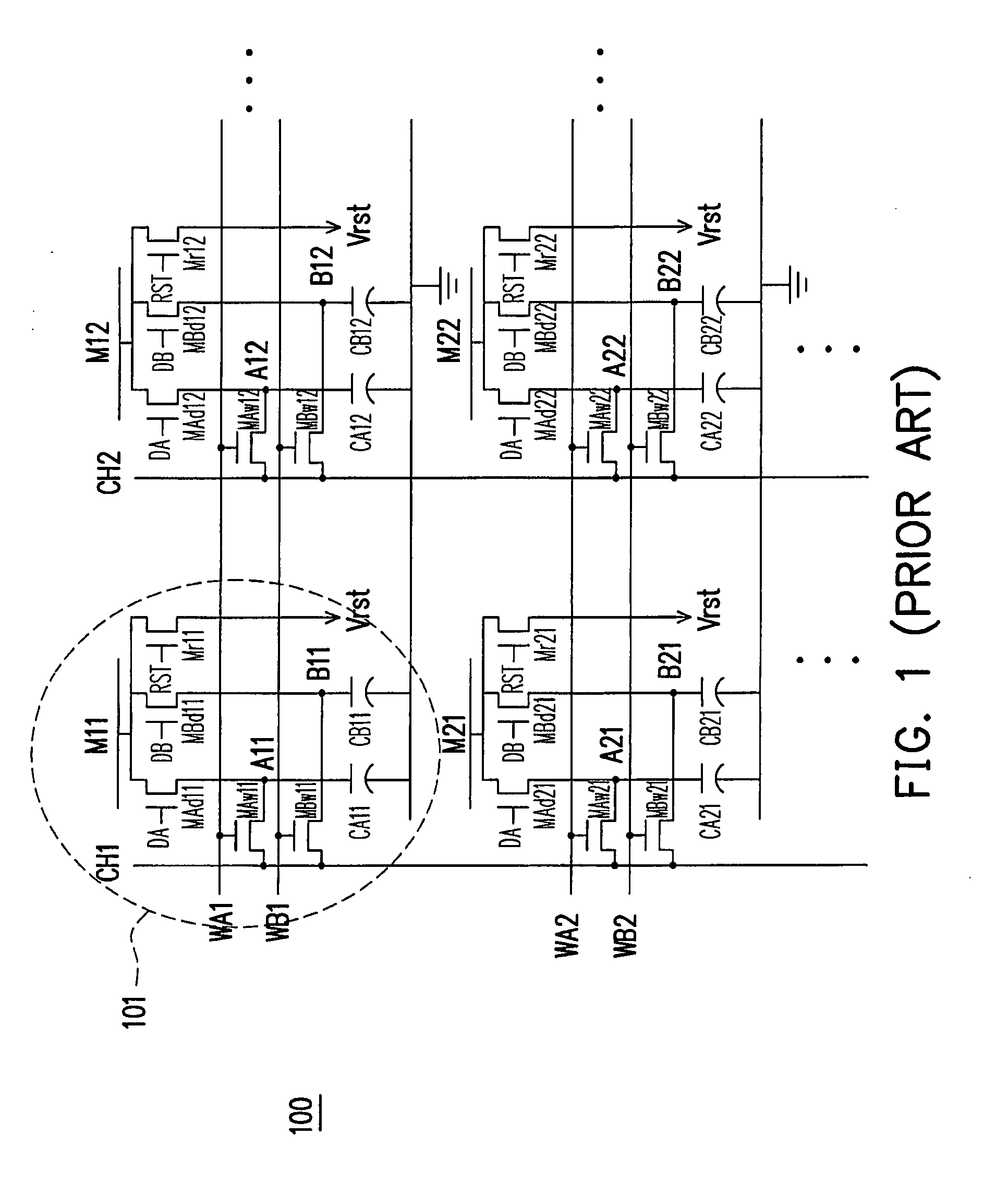
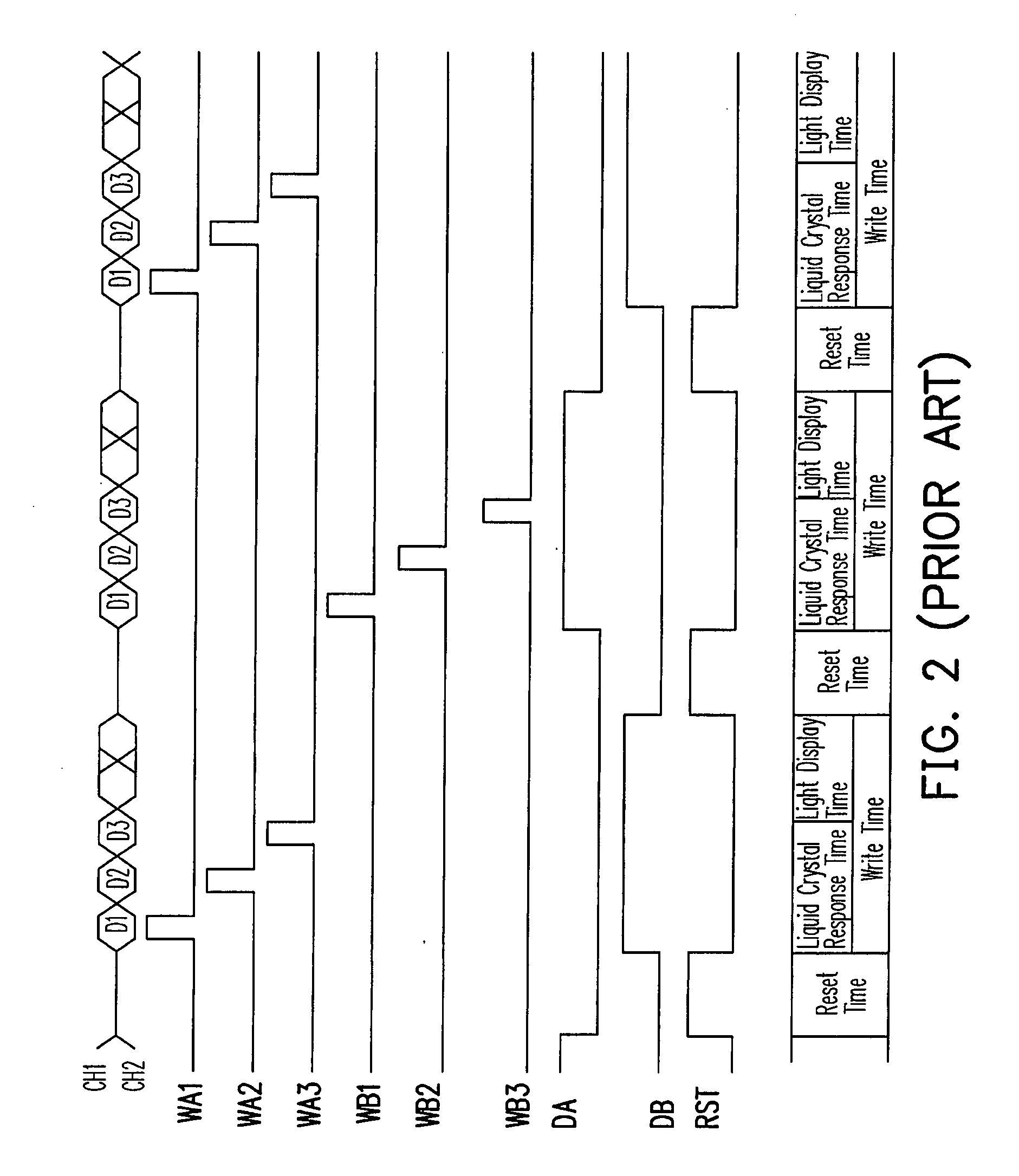
CROSS-REFERENCE TO RELATED APPLICATION[0001]This application claims the priority benefit of Taiwan application serial no. 96117571, filed May 17, 2007. All disclosure of the Taiwan application is incorporated herein by reference.BACKGROUND OF THE INVENTION[0002]1. Field of the Invention[0003]The present invention relates to a method for driving a display, and more particularly to a method for driving a liquid crystal display.[0004]2. Description of Related Art[0005]Color sequential displays have the advantages of high brightness, high resolution, and high chroma, and uses light emitting diodes (LEDs) as a light source to achieve the purpose of reduced volume and light weight. However, in order to make the images of red (R), green (G), and blue (B) overlapped to mix colors, liquid crystals with a quick response speed or a liquid crystal layer with a smaller thickness is required in processes to improve the response speed of the liquid crystal.[0006]FIG. 1 is a driving circuit diagram...

Claims


Application Information

Patent Timeline
Patent Type & Authority Applications(United States)
IPC IPC(8): G09G3/36
CPCG09G3/3659G09G2300/0814G09G2300/0842G09G2310/0235G09G2310/0251G09G2320/0219G09G2320/0252G09G2320/0257
Inventor FAN-CHIANG, KUAN-HSULIAO, BING-JEI
Owner HIMAX DISPLAY INC
Why Eureka
Eureka Blog
Learn More