Method, Apparatus and Program for Creating a Power Pin Model of a Semiconductor Integrated Circuit
- Summary
- Abstract
- Description
- Claims
- Application Information
AI Technical Summary
Benefits of technology
Problems solved by technology
Method used
Image
Examples
first embodiment
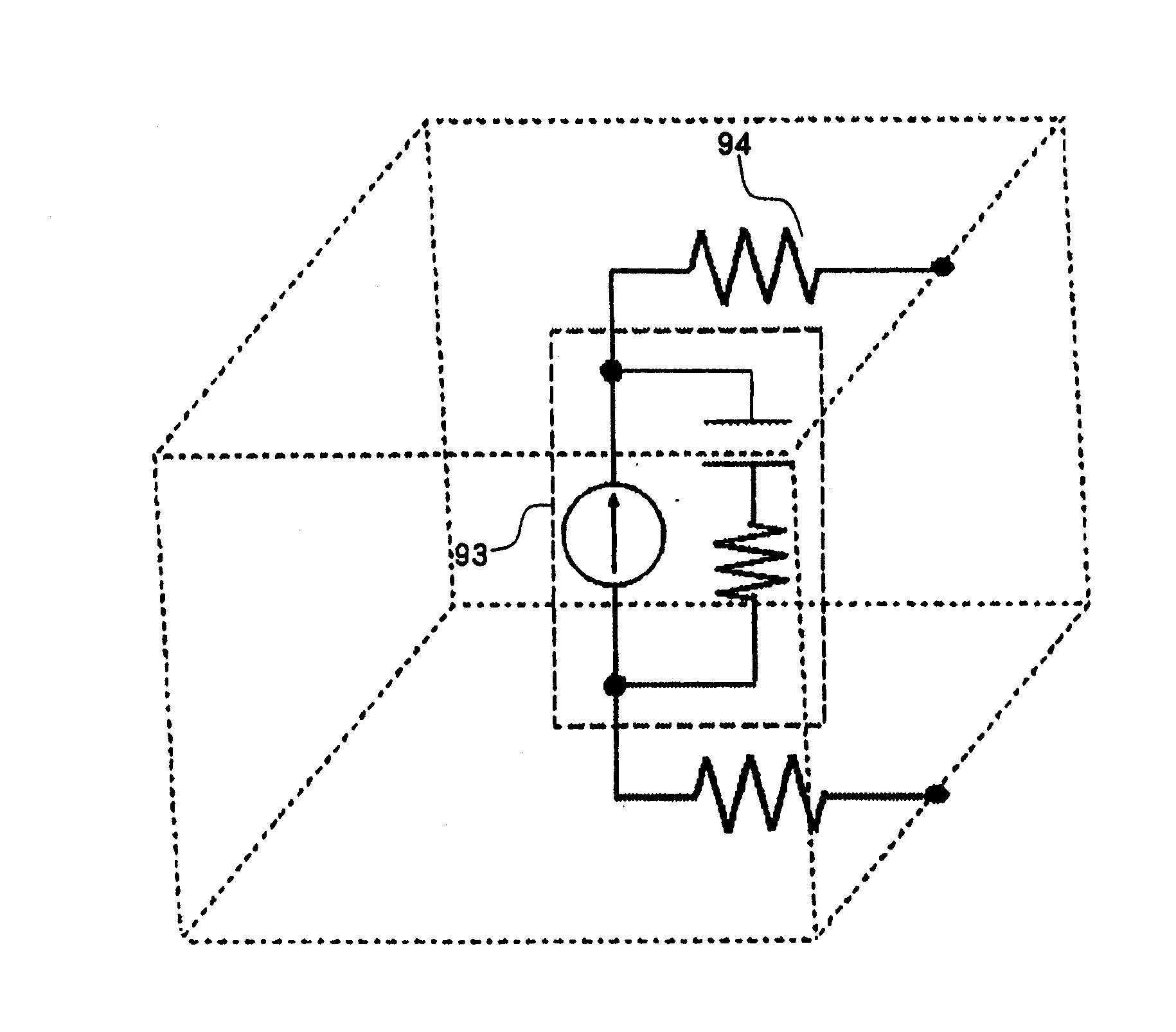
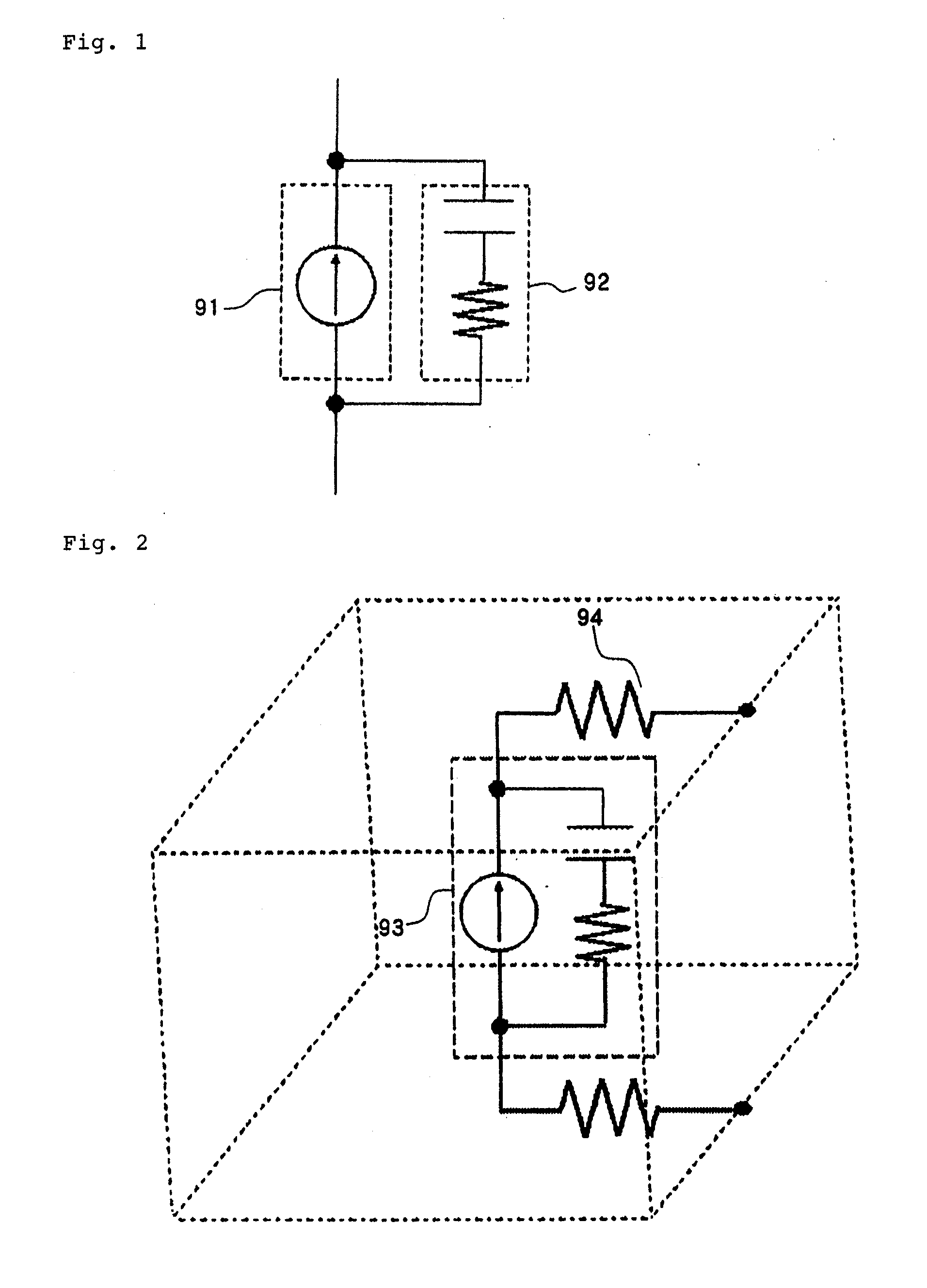
[0132]In the present embodiment, a power pin model for an LSI having only one power supply circuit network layer is created. An LSI usually has two or more types of power supplies, but in this case, it is assumed that one of the two types of power supplies is connected to ground. Active sections and internal capacitances in the LSI thus exist between the power supply circuit network layer and ground.
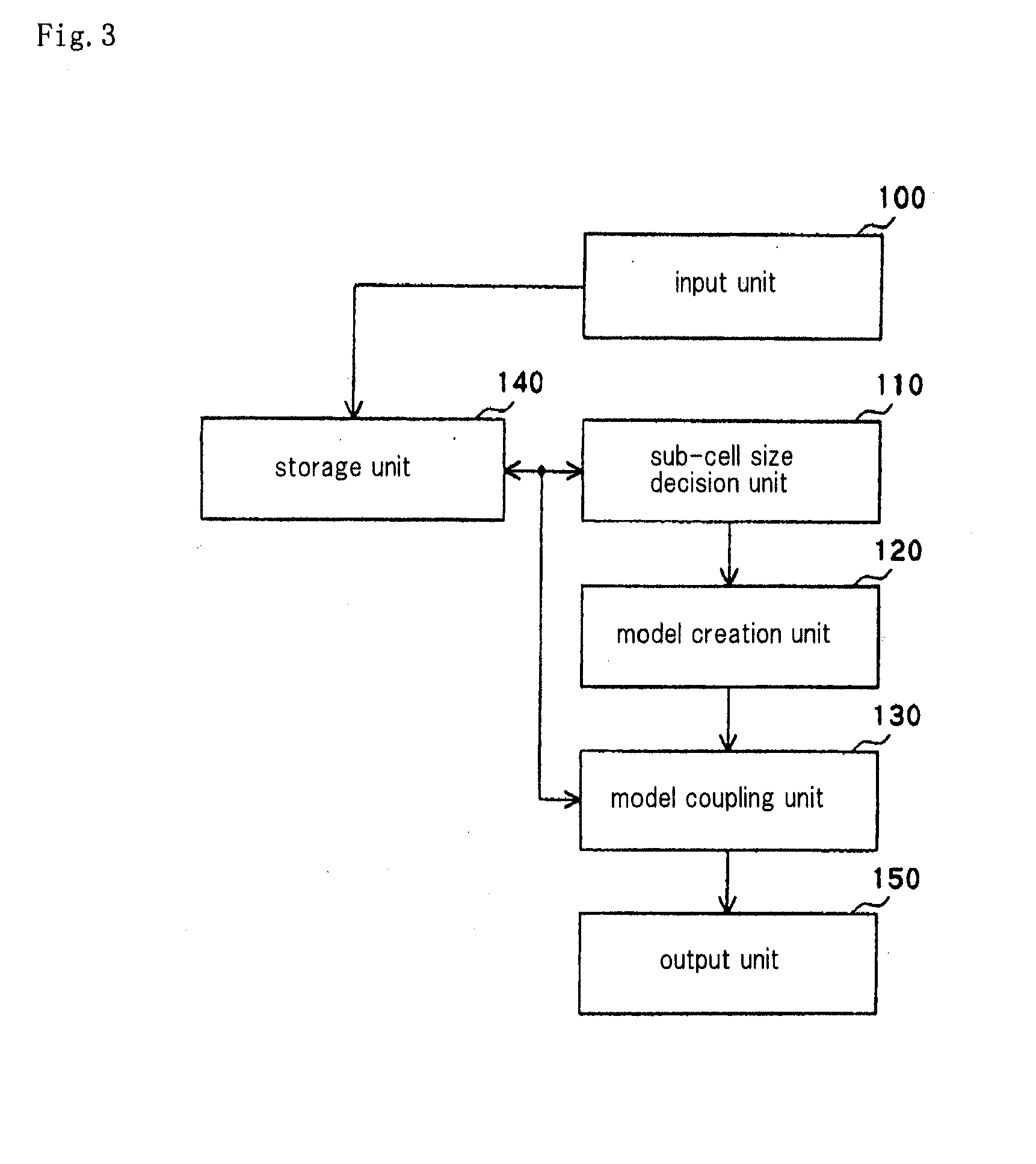
[0133]FIG. 3 is a diagram showing the configuration of a semiconductor integrated circuit power pin model creating apparatus of this embodiment. The apparatus comprises input unit 100 for entering data; divided cell size decision unit 110 for deciding the size of divided cells of an LSI; model creation unit 120 for creating a model of a power supply circuit network, a model of an active section, and a model of an internal capacitance section for each divided cell; model coupling unit 130 for coupling models for each cell to provide a power pin model of the LSI; storage unit 140 for stori...
second embodiment
[0167]In this embodiment, a description will be made of a method of creating a power pin model of a structure of an LSI having two power supply circuit network layers. In this case, an active section and an internal capacitance of the LSI exist between two types of power supply circuit network layers. Further, wires which constitute the power supply circuit network layers have respective capacitive components between them and ground. Here, the two power supply circuit network layers can be equivalently regarded as one power supply circuit network layer as shown in the first embodiment. In this case, a wiring capacitive component existing between the wire of the equivalent one power supply circuit network layer and ground is the total of the wiring capacitive components which exist between wires of the two power supply circuit network layers and ground. Accordingly, based on this idea, a power pin model of a structure having two power supply circuit network layers is created by the m...
third embodiment
[0200]In this embodiment, a description will be made of a method of creating a power pin model of an LSI in a case where there are a plurality of active sections and internal capacitance sections for the power pin model of the LSI in each cell.
[0201]FIG. 12 shows, by way of example, a power pin model for an LSI having two power supply circuit network layers in the present embodiment, the power pin model having a power pin model in each cell which includes two types of active sections. Since there are two types of active sections which perform different operations, such as different operation frequencies of the LSI, two types of active sections 34a, 34b are created. Further, since there are two types of active sections in the model of the overall LSI in semiconductor integrated circuit entire power pin model 7 of input data in FIG. 9, each active section is distributed to each cell at an appropriate proportion based on the size of each cell determined by divided cell size decision un...
PUM
 Abstract
Description
Claims
Application Information
 - R&D
- Intellectual Property
- Life Sciences
- Materials
- Tech Scout
- Unparalleled Data Quality
- Higher Quality Content
- 60% Fewer Hallucinations
Browse by: Latest US Patents, China's latest patents, Technical Efficacy Thesaurus, Application Domain, Technology Topic, Popular Technical Reports.
© 2025 PatSnap. All rights reserved.Legal|Privacy policy|Modern Slavery Act Transparency Statement|Sitemap|About US| Contact US: help@patsnap.com


