Pixel Control Device and Display Apparatus Utilizing Said Pixel Control Device
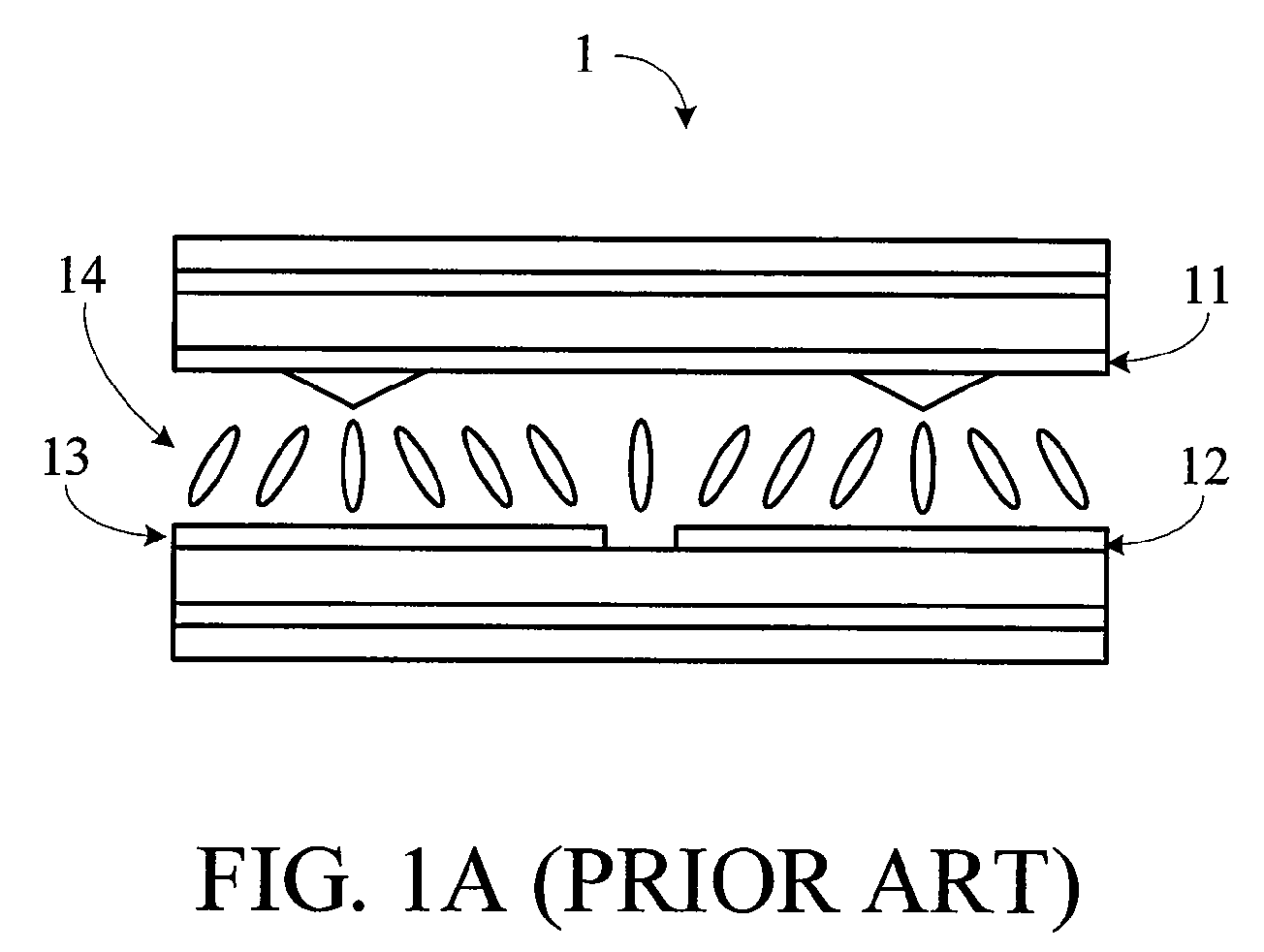
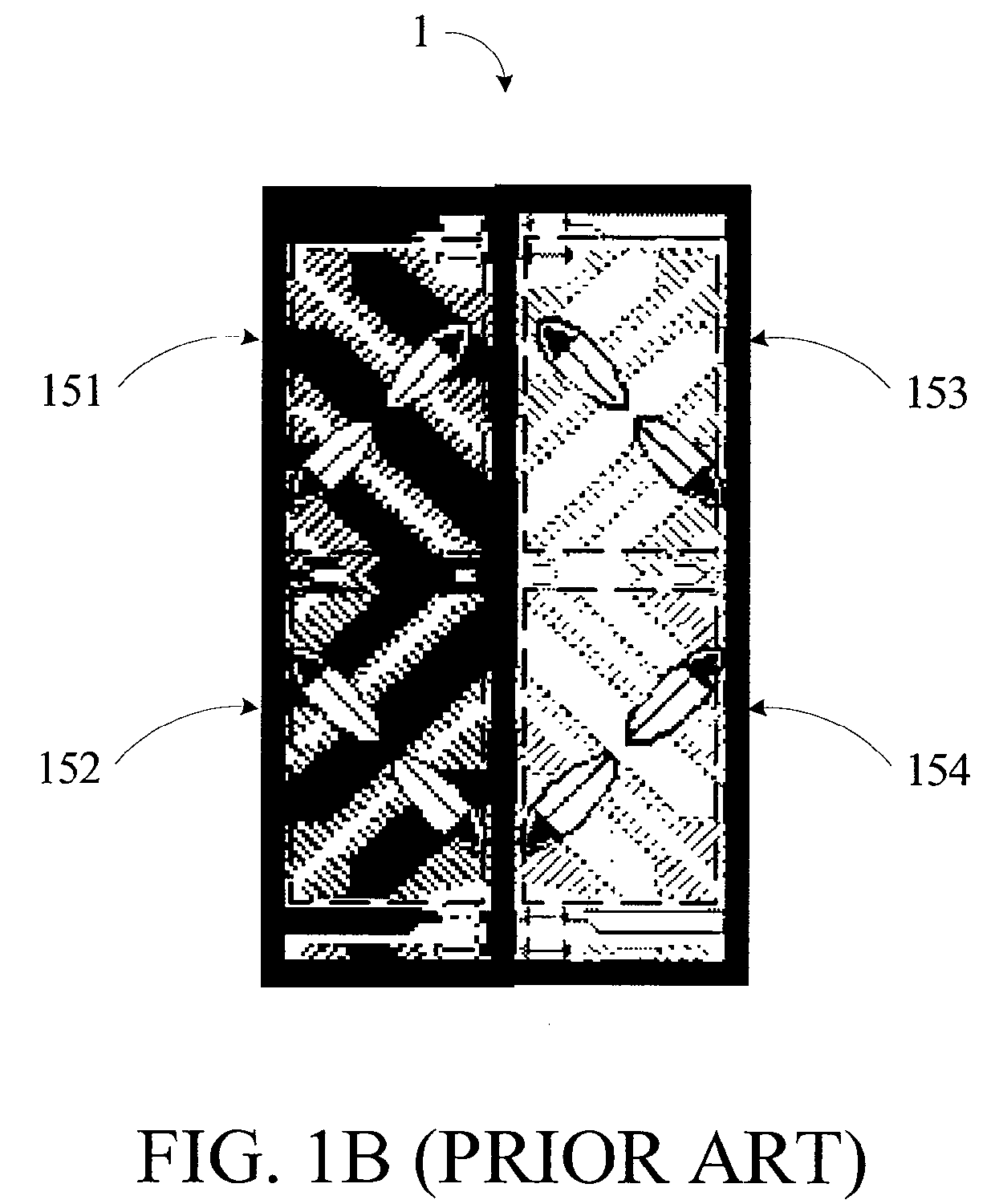
a control device and control device technology, applied in the field of pixel control devices and display devices, can solve the problems of large washout of lcd screens employing the four-domain mva technology, undesired user behavior of lcd screens, etc., and achieve the effect of preventing washout and widening the viewing angl
- Summary
- Abstract
- Description
- Claims
- Application Information
AI Technical Summary
Benefits of technology
Problems solved by technology
Method used
Image
Examples
first embodiment
[0023]FIG. 4A depicts a pixel control device 4a of a first embodiment in accordance with the present invention. The pixel control device 4a is electrically connected to a sub-pixel to provide a first voltage level, a second voltage level, and a third voltage level to the sub-pixel area.
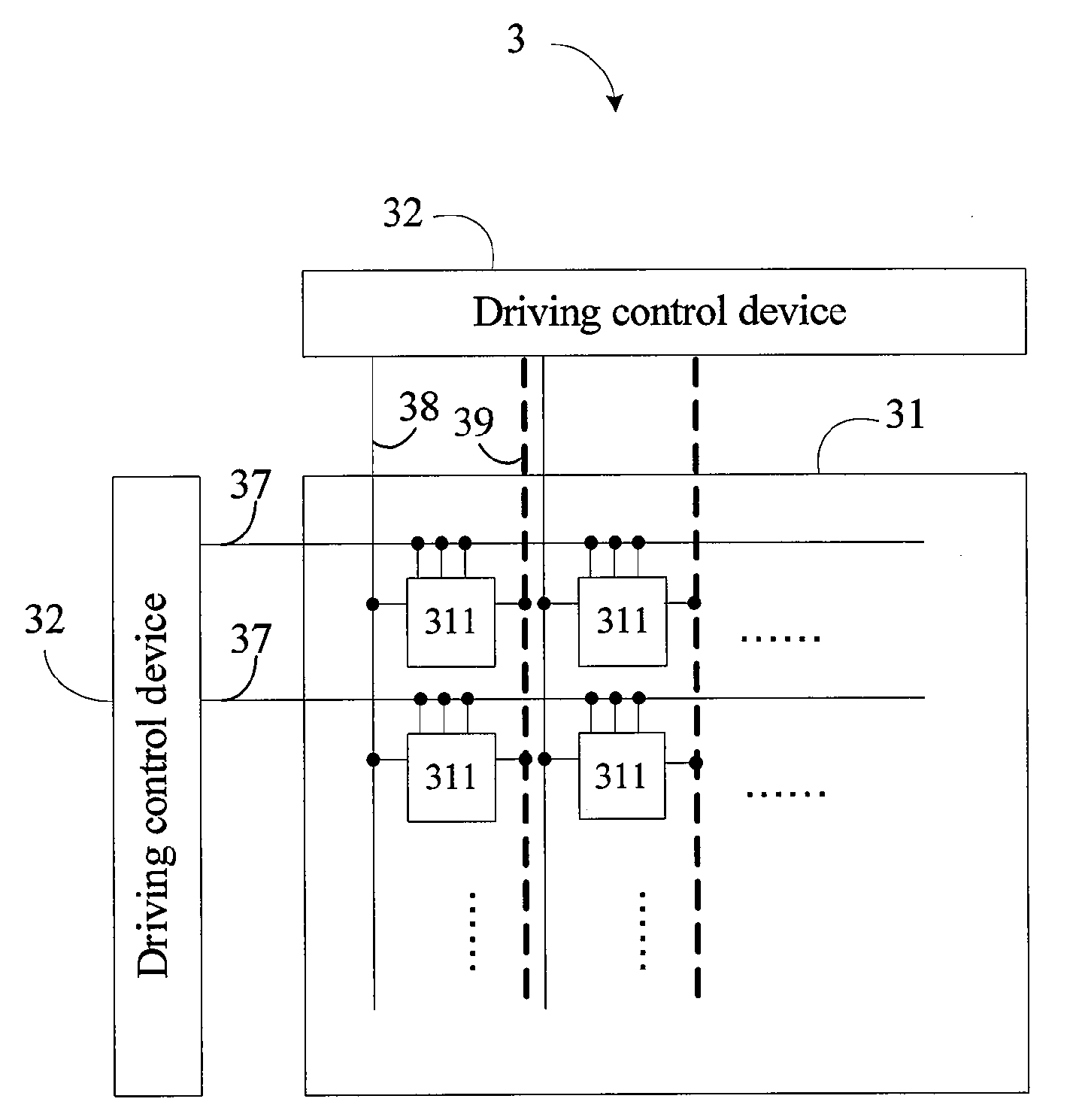
[0024]The pixel control device 4a comprises a first transistor 341, a second transistor 351, a third transistor 361, a first energy storing device 342, a second energy storing device 352, a third energy storing device 362, a first capacitor 353, a second capacitor 354, a scan line 37, a first data line 38, and a second data line 39.
[0025]The first transistor 341, the second transistor 351, and the third transistor 361 all have a gate, a source, and a drain, respectively. The respective gates of the first transistor 341, the second transistor 351, and the third transistor 361 are all coupled to the scan line 37, while the respective sources of the first transistor 341 and the second transistor 351 are ...
second embodiment
[0035]FIG. 4B depicts a pixel control device 4b of a second embodiment in accordance with the present invention. The pixel control device 4b is electrically connected to a sub-pixel to provide a first voltage level, a second voltage level, and a third voltage level to the sub-pixel.
[0036]The pixel control device 4b comprises a first transistor 341, a second transistor 351, a third transistor 361, a first energy storing device 342, a second energy storing device 352, a third energy storing device 362, a first capacitor 353, a scan line 37, a first data line 38, and a second data line 39.
[0037]The first transistor 341, the second transistor 351, and the third transistor 361 all have a gate, a source, and a drain. The respective gates of the first transistor 341, the second transistor 351, and the third transistor 361 are all coupled to the scan line 37. The respective sources of the first transistor 341 and the second transistor 351 are coupled to the first data line 38. The source of...
PUM
| Property | Measurement | Unit |
|---|---|---|
| voltage level | aaaaa | aaaaa |
| voltage | aaaaa | aaaaa |
| fixed capacitance | aaaaa | aaaaa |
Abstract
Description
Claims
Application Information
 - R&D
- Intellectual Property
- Life Sciences
- Materials
- Tech Scout
- Unparalleled Data Quality
- Higher Quality Content
- 60% Fewer Hallucinations
Browse by: Latest US Patents, China's latest patents, Technical Efficacy Thesaurus, Application Domain, Technology Topic, Popular Technical Reports.
© 2025 PatSnap. All rights reserved.Legal|Privacy policy|Modern Slavery Act Transparency Statement|Sitemap|About US| Contact US: help@patsnap.com


