Power transmission control device, power transmission device, electronic instrument, and non-contact power transmission system
a power transmission control device and control device technology, applied in the direction of instruments, inductances, transportation and packaging, etc., can solve the problem of severe resolution of determining the detected voltag
- Summary
- Abstract
- Description
- Claims
- Application Information
AI Technical Summary
Benefits of technology
Problems solved by technology
Method used
Image

Examples
first modification
5. First Modification
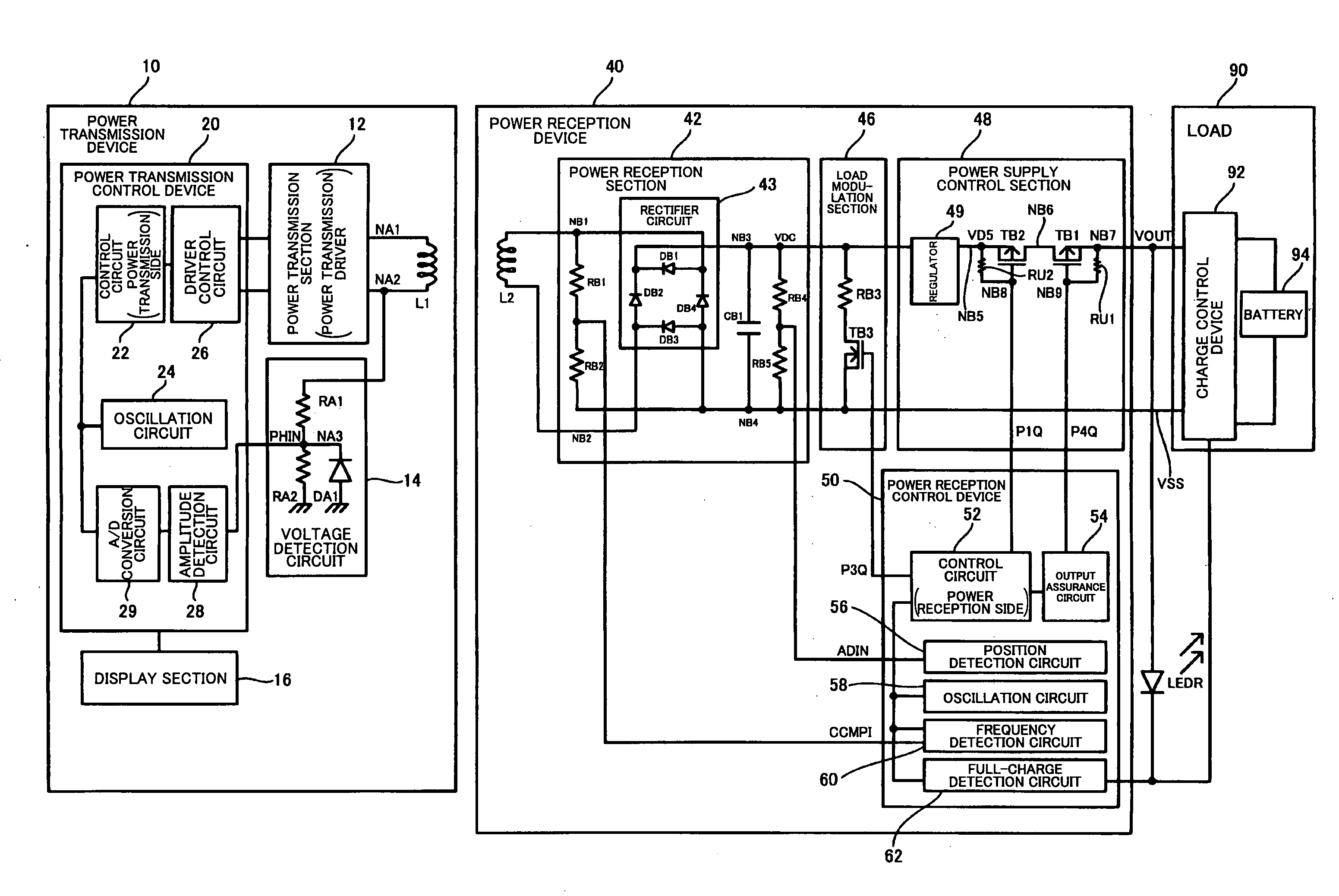
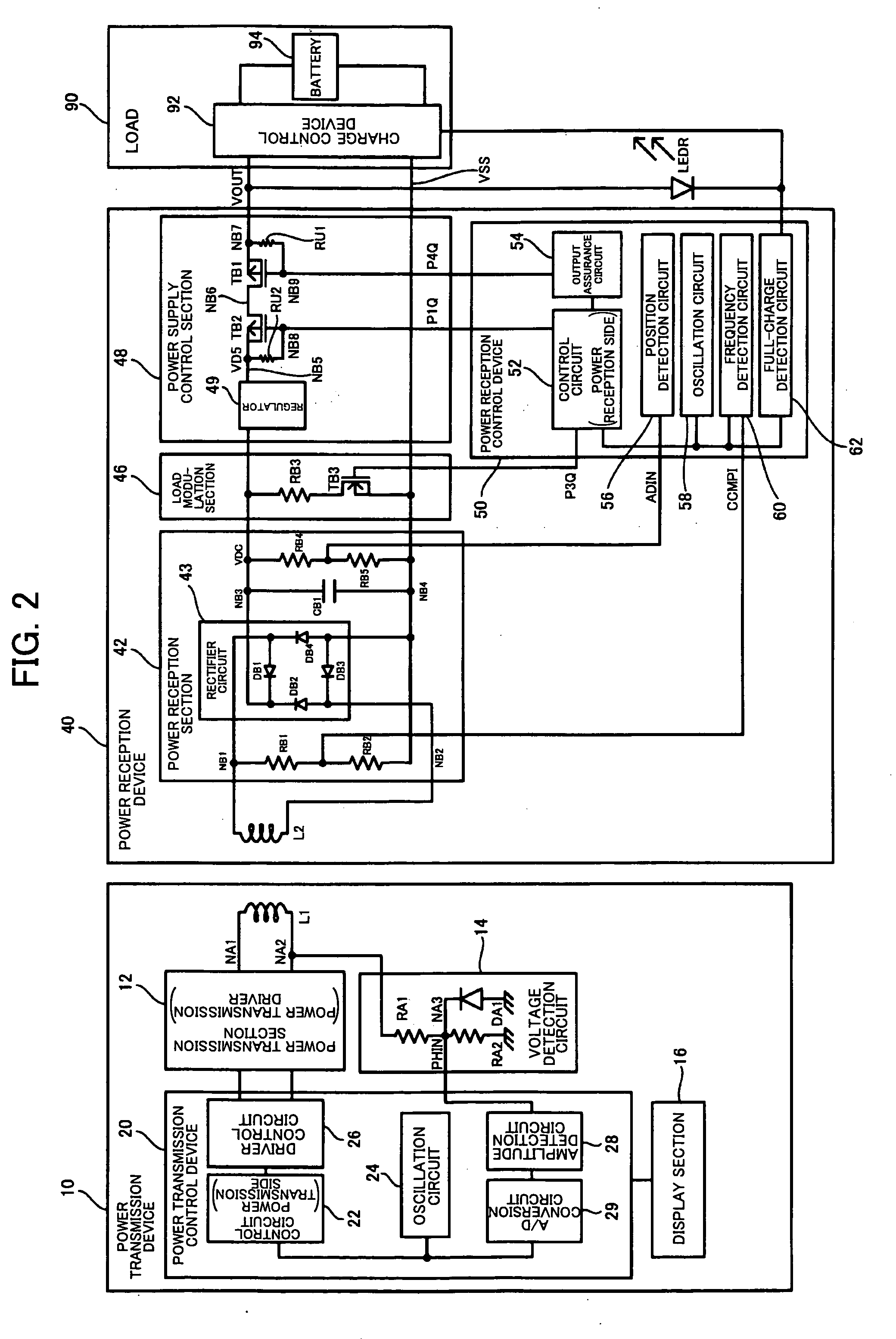
[0218]FIG. 11 shows a first modification according to this embodiment. FIG. 11 differs from FIG. 8 as to the configuration of the voltage detection circuit 14 and the addition of switch circuits SW1 and SW2.
[0219]The voltage detection circuit 14 shown in FIG. 11 includes resistors RA1, RA2, and RA3 connected in series between a node NA2 at one end of the primary coil L1 and the power supply GND (low-potential-side power supply). The resistor RA1, RA2, and RA3 form a voltage divider circuit. Induced voltage signals PHIN1 and PHIN2 (half-wave rectified signal) of the primary coil L1 are respectively output to voltage division nodes NA31 and NA32 of the voltage divider circuit. The control circuit 22 performs switching control so that the induced voltage signal from a different voltage division node is input to the amplitude detection circuit 28 during data detection and during foreign object detection / detachment detection.
[0220]Specifically, the switch circuit SW1...
second modification
6. Second Modification
[0230]FIG. 13 shows a second modification according to this embodiment. In the second modification, the pulse width of the induced voltage signal is also detected in addition to the amplitude of the induced voltage signal. FIG. 13 differs from FIG. 8 in that a waveform adjusting (shaping) circuit 32, a pulse width detection circuit 33, a latch circuit 34, and the like are added. Note that the first modification shown in FIG. 11 may be combined with the second modification shown in FIG. 13. The configuration of the second modification is not limited to FIG. 13. For example, elements such as the A / D conversion circuit 29 and the waveform adjusting circuit32 may be omitted. For example, a plurality of comparators which compare the peak voltage with the threshold voltage may be provided instead of the A / D conversion circuit 29.
[0231]The waveform adjusting circuit 32 adjusts the waveform of the induced voltage signal PHIN (coil end voltage) of the primary coil L1, a...
PUM
 Abstract
Description
Claims
Application Information
 - R&D
- Intellectual Property
- Life Sciences
- Materials
- Tech Scout
- Unparalleled Data Quality
- Higher Quality Content
- 60% Fewer Hallucinations
Browse by: Latest US Patents, China's latest patents, Technical Efficacy Thesaurus, Application Domain, Technology Topic, Popular Technical Reports.
© 2025 PatSnap. All rights reserved.Legal|Privacy policy|Modern Slavery Act Transparency Statement|Sitemap|About US| Contact US: help@patsnap.com