
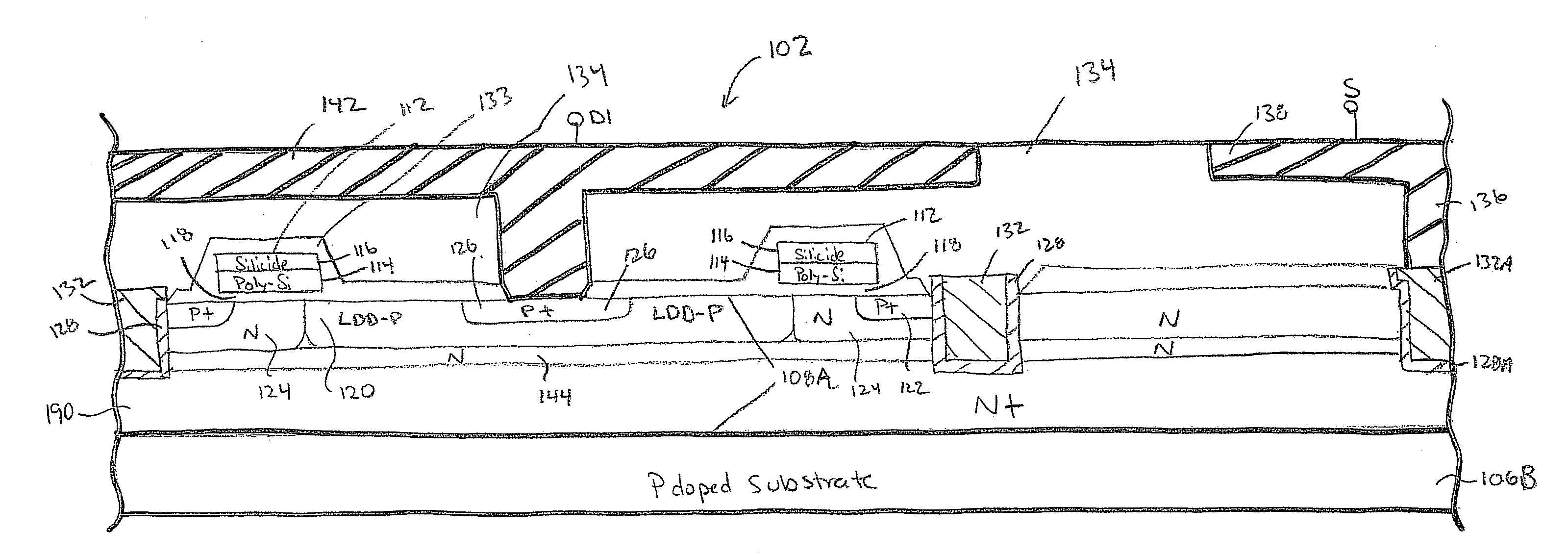
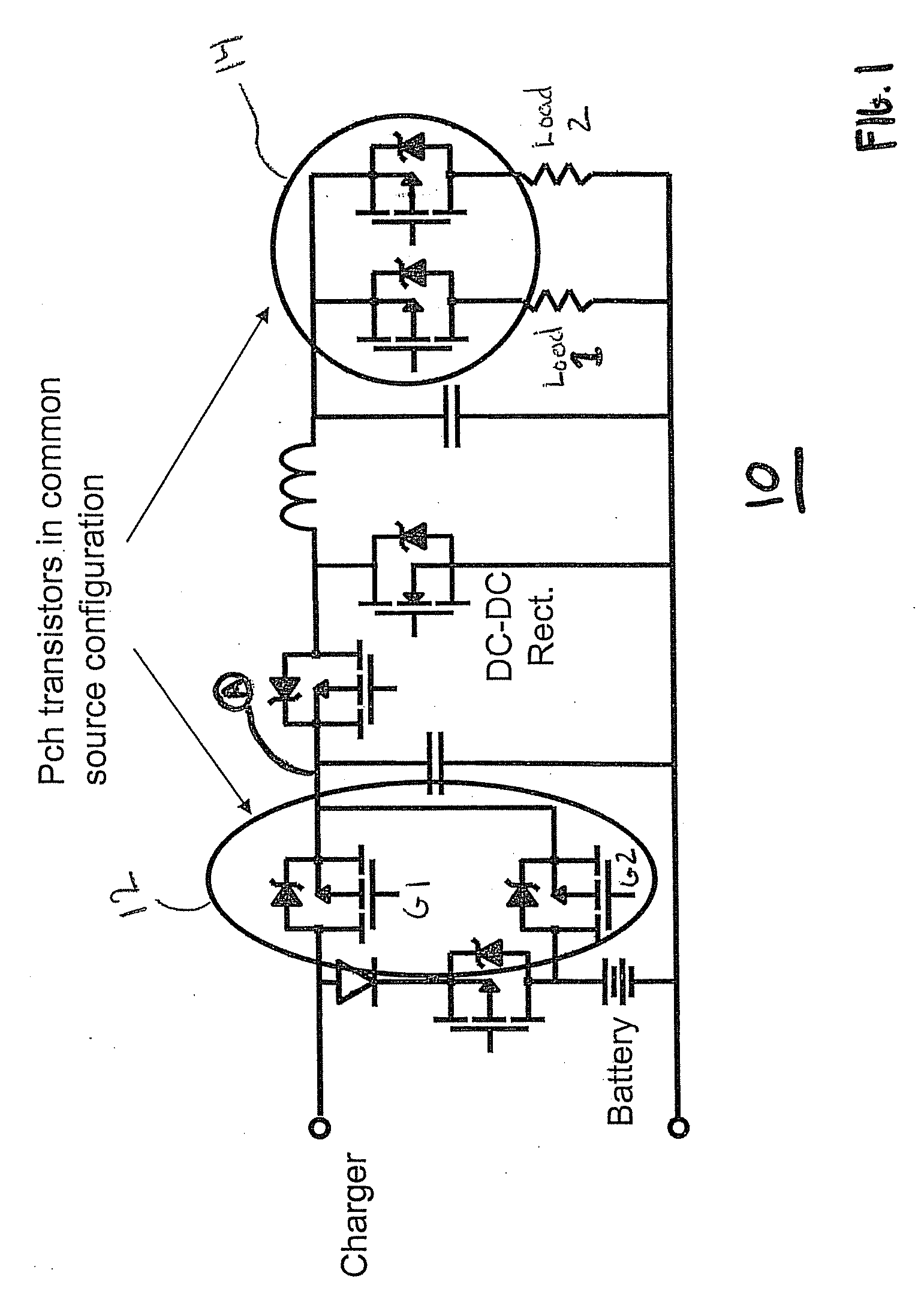
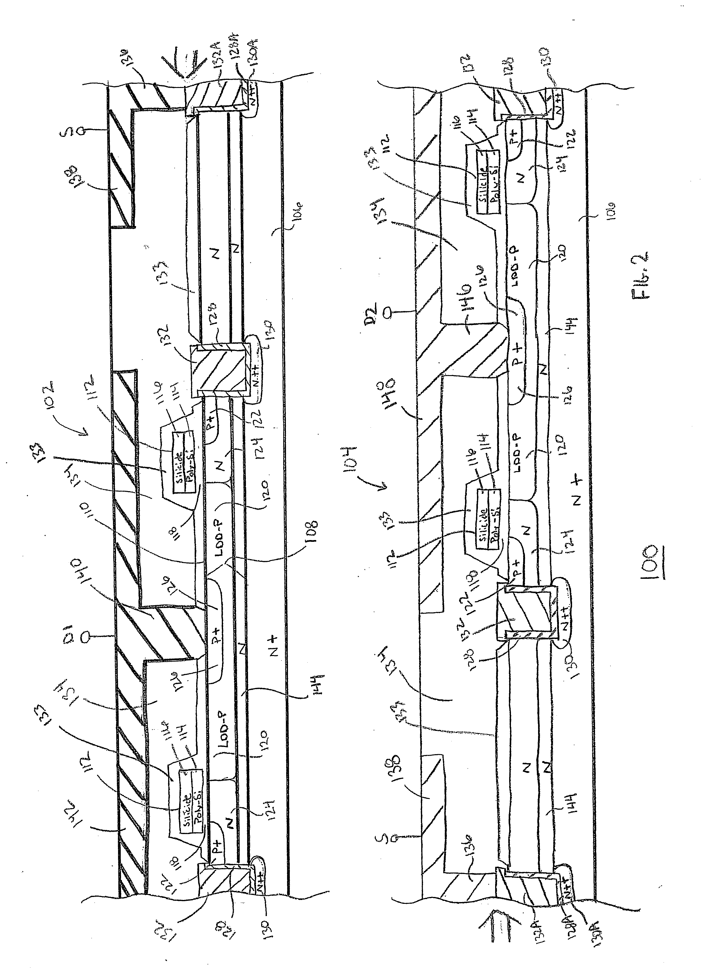
Mos transistor device in common source configuration

a transistor and common source technology, applied in the field ofmos devices, can solve the problems of 0.1v drop and devices cannot be arranged in a common source configuration

Active Publication Date: 2008-08-21
TEXAS INSTR LEHIGH VALLEY
View PDF22 Cites 69 Cited by
  • Summary
  • Abstract
  • Description
  • Claims
  • Application Information

AI Technical Summary

Problems solved by technology

A voltage drop of 0.1V is hardly acceptable.
As such, these devices cannot be arranged in a common source configuration.

Method used


Image

  • Mos transistor device in common source configuration
  • Mos transistor device in common source configuration
  • Mos transistor device in common source configuration

Examples


Embodiment Construction

[0019]This description of the exemplary embodiments is intended to be read in connection with the accompanying drawings, which are to be considered part of the entire written description. In the description, relative terms such as “lower,”“upper,”“horizontal,”“vertical,”“above,”“below,”“up,”“down,”“top” and “bottom” as well as derivative thereof (e.g., “horizontally,”“downwardly,”“upwardly,” etc.) should be construed to refer to the orientation as then described or as shown in the drawing under discussion. These relative terms are for convenience of description and do not require that the apparatus be constructed or operated in a particular orientation. Terms concerning attachments, coupling and the like, such as “connected” and “interconnected,” refer to a relationship wherein structures are secured or attached to one another either directly or indirectly through intervening structures, as well as both movable or rigid attachments or relationships, unless expressly described otherw...


PUM


Abstract

A semiconductor device includes a semiconductor substrate, a first p-channel laterally diffused metal oxide semiconductor (LDMOS) transistor formed over the semiconductor substrate and additional p-channel LDMOS transistors formed over the semiconductor substrate. First drain and gate electrodes are formed over the substrate and are coupled to the first LDMOS transistor. Additional drain and gate electrodes are formed over the substrate and are coupled to the second LDMOS transistor. A common source electrode for the first and second LDMOS transistors is also formed over the substrate.

Description

FIELD OF THE INVENTION[0001]The present invention relates to MOS devices, and more particularly to MOS devices having transistors in common source configurations.BACKGROUND OF THE INVENTION[0002]Many rechargeable, battery operated systems use common source coupled p-channel MOSFETs (PMOSs) to connect the highest available positive voltage power supply to a supply node while isolating all other power supplies, or to isolate the supply node from all power supplies. These switching elements, which are placed in series with the main current path, cannot cause an excessive voltage drop. A voltage drop of 0.1V is hardly acceptable. If a current level of 1.0 A or higher is required, the switching element must have an on-resistance (Rds,on) below 100 mΩ. Another requirement on the switching components used in battery operated portable devices is size. The components should occupy minimal area on the printed circuit board (PCB) of the device.[0003]Each of the PMOSs of a common source coupled...

Claims


Application Information

Patent Timeline
Patent Type & Authority Applications(United States)
IPC IPC(8): H01L29/74H01L29/78
CPCH01L29/41766H01L29/456H01L29/4933H01L29/7835H01L2224/16H01L2924/3025H01L2924/1305H01L2924/13091H02J9/04H01L2924/00H01L2224/05568H01L2224/05023H01L2224/05001H01L2924/00014H01L24/13H01L24/05H01L2224/0401H01L2224/05599H01L2224/05099
Inventor KOREC, JACEKCOLINO, STEPHEN L.
Owner TEXAS INSTR LEHIGH VALLEY
Learn More