Method of processing dummy pattern based on boundary length and density of wiring pattern, semiconductor design apparatus and semiconductor device

a technology of boundary length and density, which is applied in the direction of computer aided design, program control, instruments, etc., can solve the problems of changing the etching rate, reducing the effect of sidewall protective film, and breaking of wires, so as to curb the variation of wiring patterns formed and the effect of curbing the variation of wiring patterns

Active Publication Date: 2008-07-31
RENESAS ELECTRONICS CORP
View PDF4 Cites 26 Cited by
  • Summary
  • Abstract
  • Description
  • Claims
  • Application Information

AI Technical Summary

Benefits of technology

[0009]In the method of placing dummy patterns according to the present invention, the dummy patterns are placed such that the pattern density of the wiring patterns and the total value of the length of the peripheries in each divided region fall within the specified ranges. Accordingly, the pattern density of the wiring patterns and the total value of the length of the peripheries fall with

Problems solved by technology

Thus, there may occur a problem of breaking of wire and the like in a wiring layer which is formed in an upper layer.
However, the former is caused by changes in etching rate and the latter is caused by decrease in the effects of a sidewall protective film.
However, both applications, discloses no technology taking into account these causes at the same time.
Additionally, even if the method of adding dummy patterns disclosed in the first application is simply combined with the method of adding dummy patterns disclosed in the second application, the combination of the methods is not an appropriate method of adding dummy patte

Method used


Image

  • Method of processing dummy pattern based on boundary length and density of wiring pattern, semiconductor design apparatus and semiconductor device
  • Method of processing dummy pattern based on boundary length and density of wiring pattern, semiconductor design apparatus and semiconductor device
  • Method of processing dummy pattern based on boundary length and density of wiring pattern, semiconductor design apparatus and semiconductor device

Examples


first embodiment

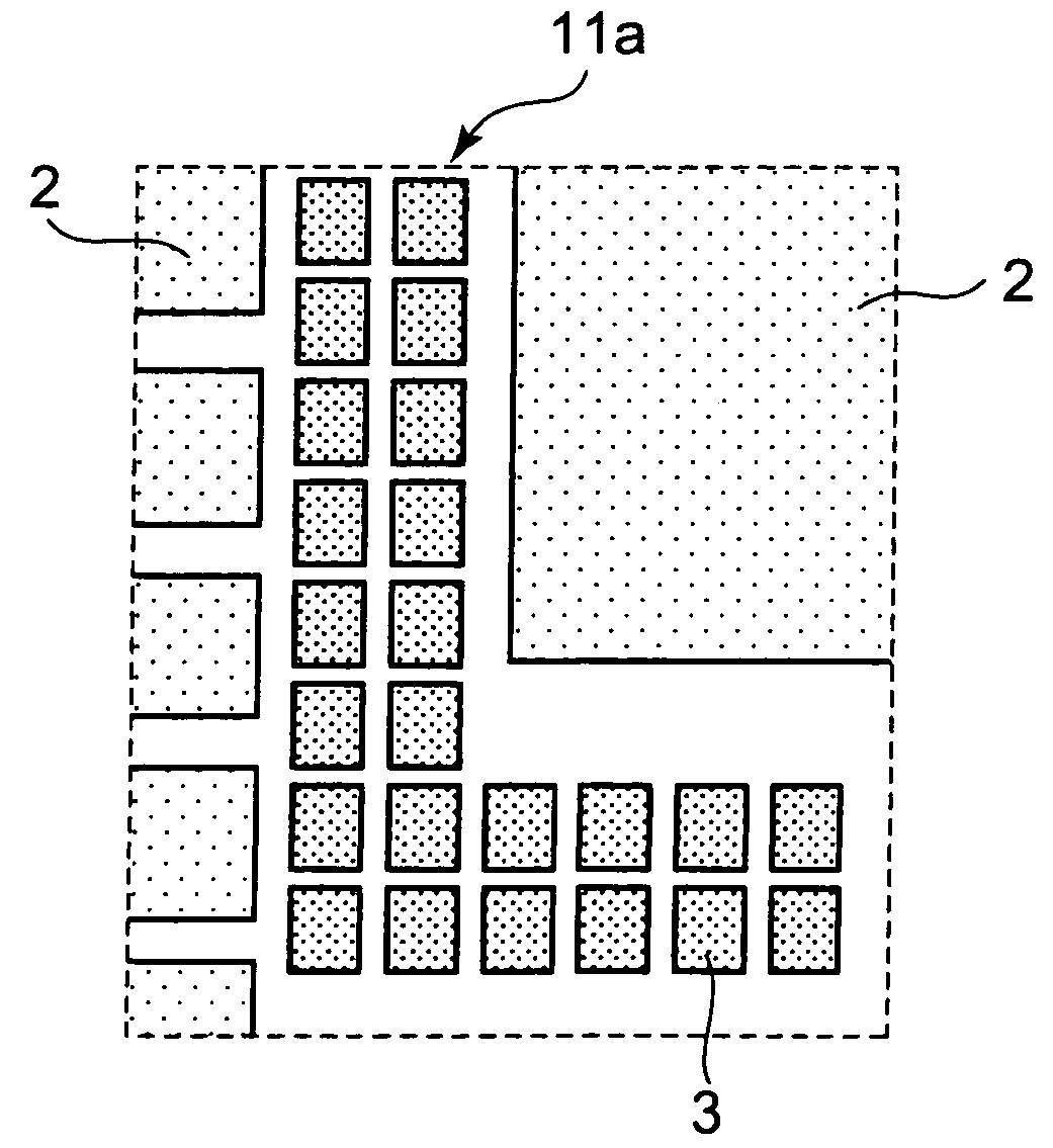
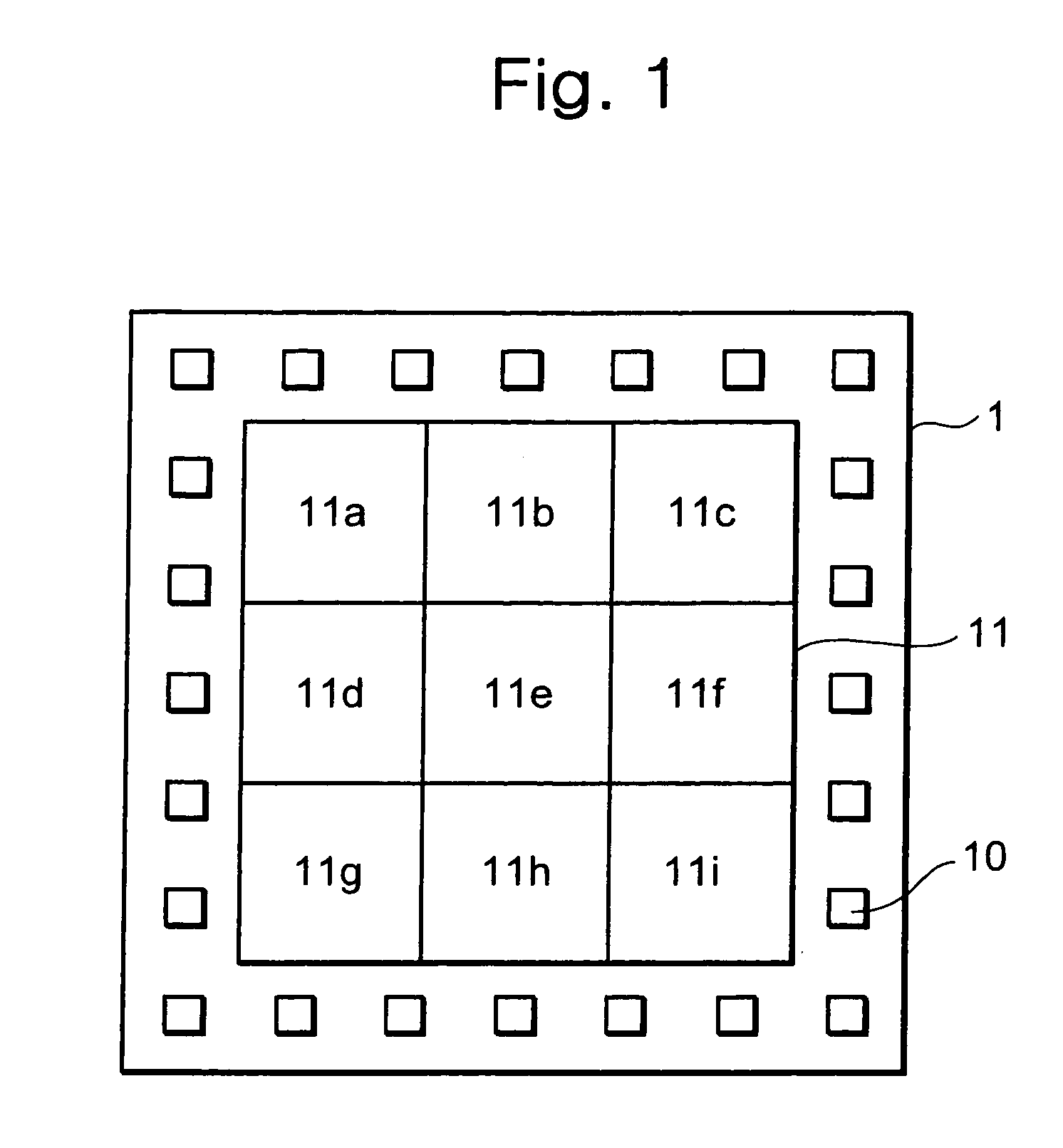
[0028]FIG. 1 shows a diagrammatic view of a semiconductor device 1 according to a first embodiment. As shown in FIG. 1, the semiconductor device 1 includes pads 10 being input / output terminals of the semiconductor device 1 and a wiring region 11 where wiring patterns of the semiconductor device 1 are formed. The wiring region 11 is divided into a plurality of divided regions 11a to 11i. The divided regions 11a to 11i are set such that each region has the same area, for example. Taking the divided regions 11a to 11d as examples out of the divided regions 11a to 11i, detailed descriptions will be given of the relation between wiring patterns and dummy patterns in a divided region. Please note that wiring patterns and dummy patterns are patterns which are formed of the same material on a semiconductor device, and are made of a metal material such as aluminum or copper.

[0029]Descriptions will be given of the divided region 11a. FIG. 2 (a) shows a diagrammatic view of layout before placi...

second embodiment

[0063]In the first embodiment, the shape of a dummy cell to be added is changed based on the density of the wiring patterns and the total value of the length of the peripheries of the wiring patterns. In contrast, a method of placing dummy patterns according to a second embodiment is to place a dummy cell in accordance with the density of the wiring patterns, and subsequently divide the placed dummy cell in accordance with the total value of the length of the peripheries of the wiring patterns in order to confine the total value of the length of the peripheries within a specified range.

[0064]FIG. 13 shows a flow chart of the method of placing dummy patterns. Please note that the descriptions will be omitted for a case where the density of the wiring patterns is within the specified range and there is no need to add dummy cells. In the flow of placing dummy patterns according to the second embodiment, data collected after laying wiring patterns out, when the placement of wiring patte...


PUM


Abstract

A method of placing a dummy pattern in a wiring region includes calculating a density of a wiring pattern in the wiring region and calculating a value of a length of a periphery of the wiring pattern. The dummy pattern is then set such that a total of the pattern density and the value of the length of the periphery of the wiring pattern and the dummy pattern in the wiring region falls within specified ranges in the wiring region.

Description

BACKGROUND OF THE INVENTION[0001]1. Field of the Invention[0002]The present invention relates to a method of placing dummy patterns, a semiconductor design apparatus and a semiconductor device, and particularly relates to a method of placing dummy patterns, a semiconductor design apparatus and a semiconductor device, which curb variations in the total length of the peripheries of wiring patterns and dummy patterns in a chip.[0003]2. Description of Related Art[0004]In recent years, semiconductor devices have been advancing toward multilayer wiring. With multilayer wiring, the high level the wiring layer is, the larger the unevenness of a plane where the wiring is formed becomes. Thus, there may occur a problem of breaking of wire and the like in a wiring layer which is formed in an upper layer. Accordingly, a technology is known of placing dummy patterns in a region where a wiring pattern is not formed and reducing the unevenness of the wiring layer in order to increase reliability i...

Claims


Application Information

Patent Timeline
IPC IPC(8): H01L23/52G06F17/50
CPCG06F17/5077H01L2224/05554H01L24/06H01L23/522G06F30/394
Inventor HIRABAYASHI, KEISUKE
Owner RENESAS ELECTRONICS CORP
Why Eureka
Try Eureka