
Pixel sensor cell having asymmetric transfer gate and method of forming

Inactive Publication Date: 2008-07-31
IBM CORP
View PDF1 Cites 31 Cited by
  • Summary
  • Abstract
  • Description
  • Claims
  • Application Information

AI Technical Summary

Benefits of technology

[0010]The invention addresses a novel pixel sensor cell structure and method of manufacture. Particularly, a novel pixel sensor cell is fabricated whereby a potential barrier between the charge collection well and the transfer gate channel is reduced without adversely affecting the performance of the photodiode and the transfer gate.
[0011]According to a first aspect of the invention, there is provided a pixel sensor cell comprising an asymmetric transfer gate formed on a substrate. A photosensitive region (e.g. photodiode) is formed adjacent a first side of the asymmetric transfer gate including a charge collection well having an edge substantially defined by a first feature of the asymmetric transfer gate and a pinning layer having an edge substantially defined by a second feature of the asymmetric transfer gate. The edge of the pinning layer is spaced a distance further away from a channel region of the asymmetric transfer gate than the edge of the collection well region. This improves the control of the readout of the charge of the pixel sensor cell as the ability of the pinning layer to produce a potential barrier to charge transfer is reduced without adversely affecting the performance of the photodiode and the transfer gate.

Problems solved by technology

A problem with these current CMOS imaging cells with a charge transfer gate 25 (e.g., a “4 Transistor” cell) is the definitional problem of controlling the readout of the charge.

Method used


Image

  • Pixel sensor cell having asymmetric transfer gate and method of forming
  • Pixel sensor cell having asymmetric transfer gate and method of forming
  • Pixel sensor cell having asymmetric transfer gate and method of forming

Examples


Embodiment Construction

[0018]Embodiments of the invention are described herein below in terms of a “pixel sensor cell”. It is noted that the term “pixel sensor cell” is used to generally refer to any type of sensor cell which is capable of converting incident electromagnetic radiation into an electrical signal. An example of a pixel sensor cell according to the invention includes a pixel sensor cell that is capable of detecting optical wavelengths of electromagnetic radiation and is commonly referred to as an “image sensor”. An image sensor fabricated using CMOS technology is commonly referred to as a “CMOS image sensor”.

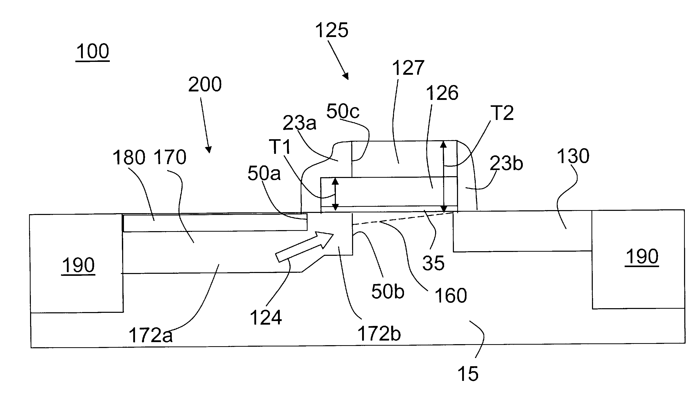
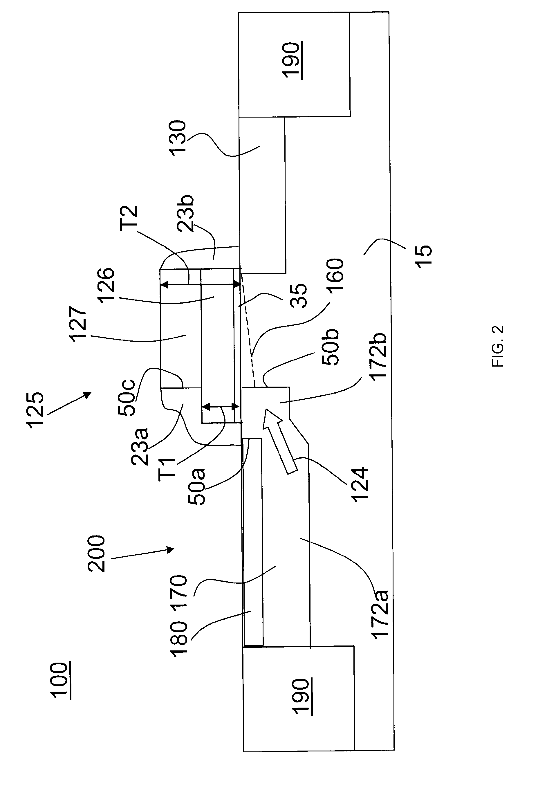
[0019]FIG. 2 illustrates a pixel sensor cell 100 according to an embodiment of the present invention. As shown in FIG. 2, pixel sensor cell 100 includes a transfer gate 125 on top of a gate dielectric material layer 35 which is formed on a surface of a semiconductor substrate 15. Gate sidewall spacer 23a, 23b is formed adjacent to sides of transfer gate 125. Between one side of transfer g...


PUM


Abstract

A pixel sensor cell structure and method of manufacture. Disclosed is a pixel sensor cell comprising an asymmetric transfer gate for providing a pinning layer having an edge spaced a further distance from the gate channel region than an edge of a charge collection well. Potential barrier interference to charge transfer caused by the pinning layer is reduced.

Description

CROSS REFERENCE TO RELATED APPLICATIONS[0001]The present invention is related to commonly-owned co-pending U.S. patent application Ser. No. 10 / 905,097 filed Dec. 15, 2004 and entitled “A RECESSED GATE FOR AN IMAGE SENSOR”, and U.S. patent application Ser. No. 10 / 907,570 filed Apr. 6, 2005 and entitled “PIXEL SENSOR CELL HAVING REDUCED PINNING LAYER BARRIER POTENTIAL AND METHOD THEREOF”, the whole contents and disclosures of which are incorporated by reference as if fully set forth herein.FIELD OF THE INVENTION[0002]The present invention relates generally to semiconductor devices and a method of forming semiconductor devices, and more particularly, to a semiconductor pixel sensor cell and method of forming the semiconductor pixel sensor cell.BACKGROUND OF THE INVENTION[0003]CMOS image sensors are beginning to replace conventional CCD sensors for applications requiring image pick-up such as digital cameras, cellular phones, PDA (personal digital assistant), personal computers, and the...

Claims


Application Information

Patent Timeline
IPC IPC(8): H01L31/113
CPCH01L27/14603H01L27/1463H01L27/14609
Inventor GAMBINO, JEFFREYJAFFE, MARK
Owner IBM CORP
Learn More