Microfabricated Cell Sorter
a sorter and microfabricated technology, applied in the field of microfabricated devices, can solve the problems of many failures of these instruments, high failure rate of these instruments, and high failure rate of these instruments, and achieve the effect of high sorting rate of droplet generation and electrical charging
- Summary
- Abstract
- Description
- Claims
- Application Information
AI Technical Summary
Benefits of technology
Problems solved by technology
Method used
Image
Examples
example 1
Microfabrication of a Silicon Device
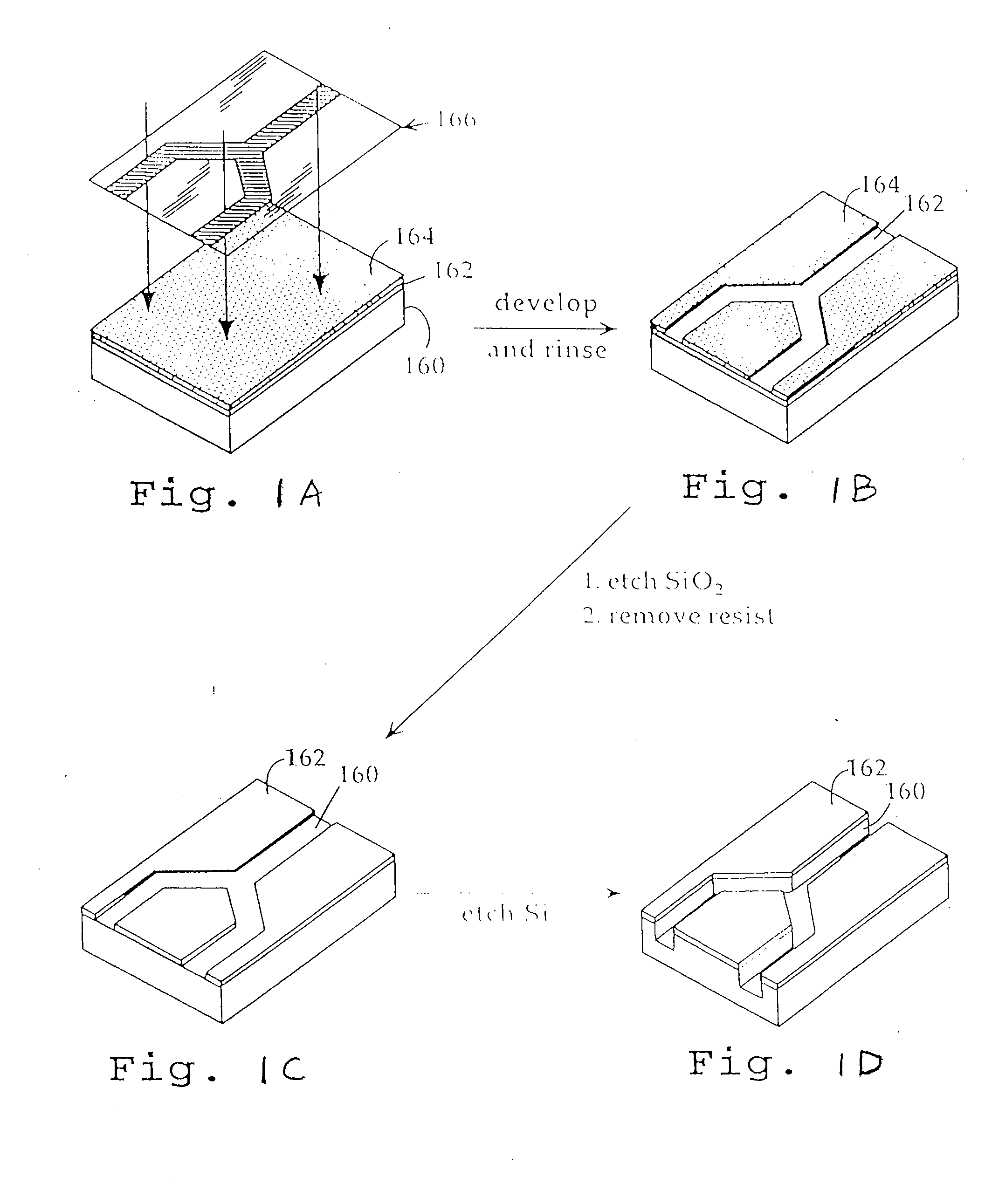
[0081]Analytical devices having microscale flow channels, valves and other elements can be designed and fabricated from a solid substrate material. Silicon is a preferred substrate material due to well-developed technology permitting its precise and efficient fabrication, but other materials may be used, including polymers such as polytetrafluoroethylenes. Micromachining methods well known in the art include film deposition processes, such as spin coating and chemical vapor deposition, laser fabrication or photolithographic techniques, or etching methods, which may be performed by either wet chemical or plasma processes. See, e.g., (37) and (38).
[0082]FIGS. 1A-1D illustrate the initial steps in microfabricating the channels and discrimination region of a cell sorting device of the invention by photolithographic techniques. As shown, the structure includes a silicon substrate 160. The silicon wafer which forms the substrate is typically washed in a...
example 2
Photodiode Detectors
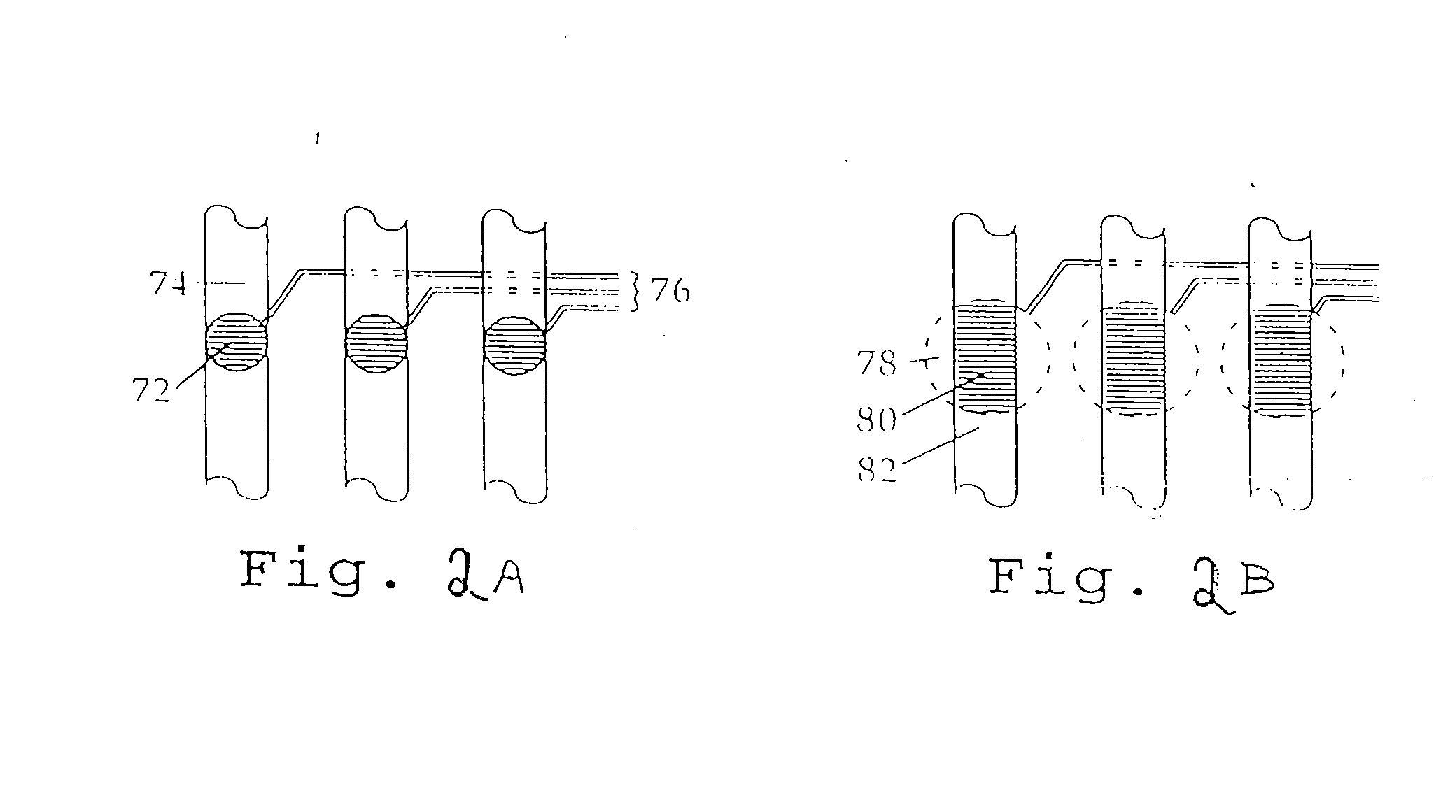
[0087]In one embodiment of the invention, shown in FIG. 2A, each detection region is formed from a portion of a channel 74 of an analysis unit and includes a photodiode 72 preferably located in the floor of the main channel. The detection region encompasses a receptive field of the photodiode in the channel, which receptive field has a circular shape. The volume of the detection region is the volume of a cylinder with a diameter equal to the receptive field of the photodiode and a height equal to the depth of the channel above the photodiode.
[0088]The signals from the photodiodes 72 can be carried to a processor via one or more lines 76, representing any form of electrical communication (including e.g. wires, conductive lines etched in the substrate, etc.). The processor acts on the signals, for example by processing them into values for comparison with a predetermined set of values for sorting the cells. In one embodiment, the values correspond to the amount of ...
example 3
Valve Structures
[0095]In an embodiment where pressure separation is used for discrimination of cells, valves can be used to block or unblock the pressurized flow of cells through selected channels. A thin cantilever, for example, may be included within a branch point, as shown in FIGS. 3A and 3B, such that it may be displaced towards one or the other wall of the main channel, typically by electrostatic attraction, thus closing off a selected branch channel. Electrodes are on the walls of the channel adjacent to the end of the cantilever. Suitable electrical contacts for applying a potential to the cantilever are also provided in a similar manner as the electrodes.
[0096]A valve within a channel may be microfabricated, if desired, in the form of an electrostatically operated cantilever or diaphragm. Techniques for forming such elements are well known in the art (e.g., 24, 29, 35, 36, 37). Typical processes include the use of selectively etched sacrificial layers in a multilayer struct...
PUM
| Property | Measurement | Unit |
|---|---|---|
| volume | aaaaa | aaaaa |
| volume | aaaaa | aaaaa |
| volume | aaaaa | aaaaa |
Abstract
Description
Claims
Application Information
 - R&D
- Intellectual Property
- Life Sciences
- Materials
- Tech Scout
- Unparalleled Data Quality
- Higher Quality Content
- 60% Fewer Hallucinations
Browse by: Latest US Patents, China's latest patents, Technical Efficacy Thesaurus, Application Domain, Technology Topic, Popular Technical Reports.
© 2025 PatSnap. All rights reserved.Legal|Privacy policy|Modern Slavery Act Transparency Statement|Sitemap|About US| Contact US: help@patsnap.com


