
Method for manufacturing organic light emitting display

a technology of organic light and display, which is applied in the manufacture of electrode systems, lighting and heating apparatuses, electric discharge tubes/lamps, etc., can solve the problems of deteriorating test performance, inability to perform sheet test, and surface of test wiring

Active Publication Date: 2008-07-03
SAMSUNG DISPLAY CO LTD
View PDF2 Cites 28 Cited by
  • Summary
  • Abstract
  • Description
  • Claims
  • Application Information

AI Technical Summary

Problems solved by technology

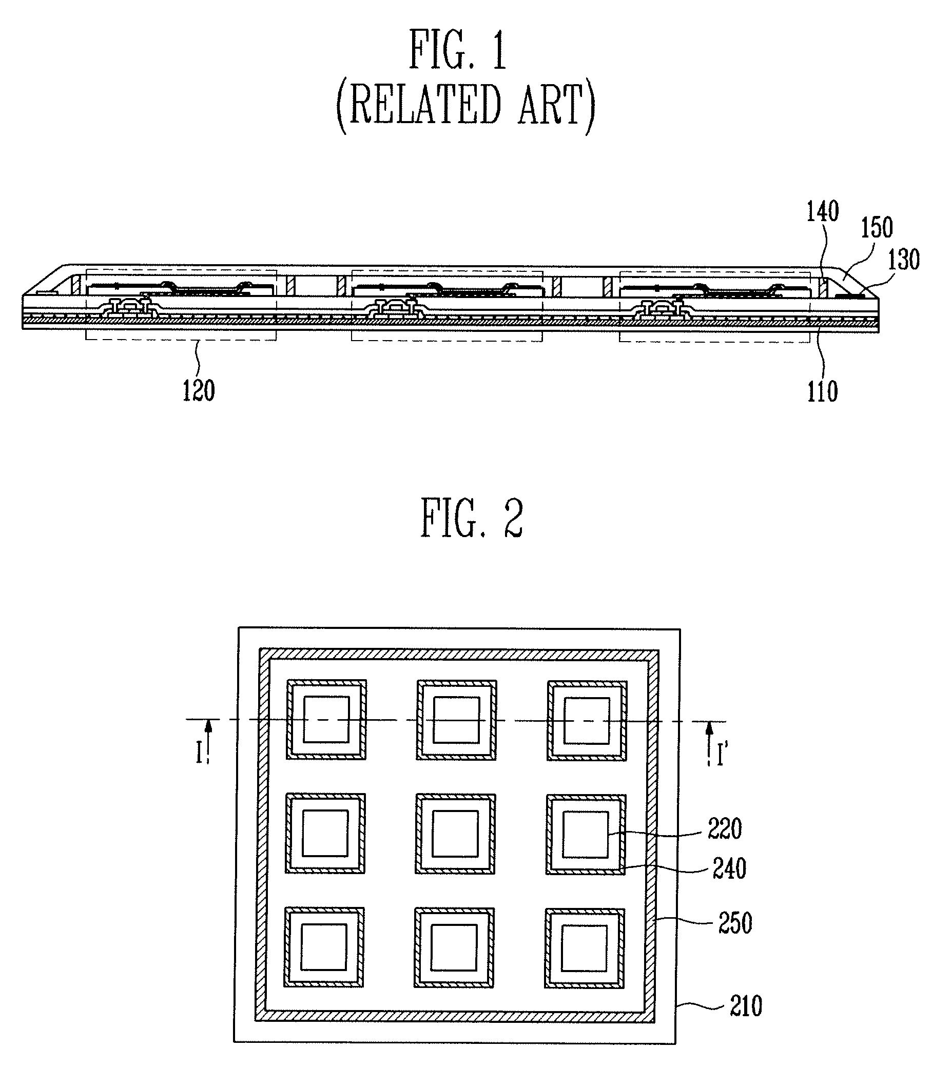
Further, because the panels should be separately tested, a performance of the test is deteriorated.
Accordingly, when the sealing substrate 150 formed at an upper portion of the test wiring 130 is scribed and removed, a surface of the test wiring 130 is damaged, with the result that a sheet test cannot be performed.

Method used


Image

  • Method for manufacturing organic light emitting display
  • Method for manufacturing organic light emitting display
  • Method for manufacturing organic light emitting display

Examples


Embodiment Construction

[0034]In the following detailed description, only certain exemplary embodiments of the present invention have been shown and described, simply by way of illustration. As those skilled in the art would realize, the described embodiments may be modified in various different ways, all without departing from the spirit or scope of the present invention. Accordingly, the drawings and description are to be regarded as illustrative in nature and not restrictive. In addition, when an element is referred to as being “on” another element, it can be directly on the another element or be indirectly on the another element with one or more intervening elements interposed therebetween. Also, when an element is referred to as being “connected to” another element, it can be directly connected to the another element or be indirectly connected to the another element with one or more intervening elements interposed therebetween. Hereinafter, like reference numerals refer to like elements.

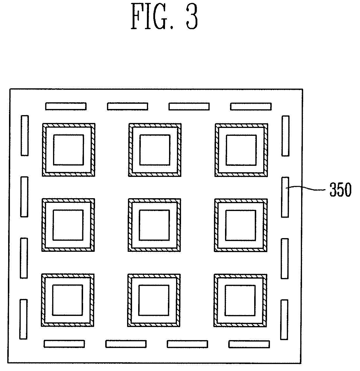
[0035]FIG. 2 i...


PUM

PropertyMeasurementUnit
flexibleaaaaaaaaaa
sizeaaaaaaaaaa
voltageaaaaaaaaaa

Abstract

A method for manufacturing an organic light emitting display. Pixel portions are formed on a mother substrate. A test wiring for testing pixel portions is formed at a peripheral portion of the mother substrate. A sealing material is formed at one surface of a sealing substrate to enclose the pixel portions, the sealing substrate being sealed to be spaced apart from the mother substrate. A spacer is formed at a side region of the one surface of the sealing substrate on which the sealing material is formed. The mother substrate and the sealing substrate are adhered to each other by the sealing material to seal the pixel portions within an enclosure formed by the mother substrate, sealing surface, and sealing material. A part of the sealing substrate is scribed and removed to expose the test wiring, the part of sealing substrate being arranged over a portion of the test wiring.

Description

CROSS-REFERENCE TO RELATED APPLICATIONS[0001]This application claims priority to and the benefit of Korean Patent Application No. 10-2007-0000637, filed on Jan. 3, 2007, and No. 10-2007-0009701, filed on Jan. 30, 2007, in the Korean Intellectual Property Office, the entire contents of which are incorporated herein by reference.BACKGROUND[0002]1. Field of the Invention[0003]The present invention relates to a method for manufacturing an organic light emitting display.[0004]2. Discussion of Related Art[0005]In general, after a plurality of pixel portions in an organic light emitting display are formed on a substrate, they are scribed to divide into separate panels. A method for testing whether or not panels are defective can be divided into testing types.[0006]In a first testing type, after a substrate is scribed into separate panels, the panels are separately tested. However, in this testing type, if a circuit wiring forming a panel or a size of the panel varies, testing equipment or ...

Claims


Application Information

Patent Timeline
Patent Type & Authority Applications(United States)
IPC IPC(8): H01J9/26
CPCH01L27/3276H01L51/56H01L51/5237H10K59/131H10K71/70H10K59/8723H10K59/871H10K71/40H10K59/8722H10K50/8428H10K50/841H10K71/00
Inventor SONG, SEUNG-YONGCHOI, YOUNG-SEOLEE, KWAN-HEEJUNG, SUN-YOUNGKWON, OH-JUNEZU, YOUNG-CHEOLRYU, JI-HUN
Owner SAMSUNG DISPLAY CO LTD
Learn More