Intra-pixel convolution for amoled
- Summary
- Abstract
- Description
- Claims
- Application Information
AI Technical Summary
Benefits of technology
Problems solved by technology
Method used
Image
Examples
first embodiment
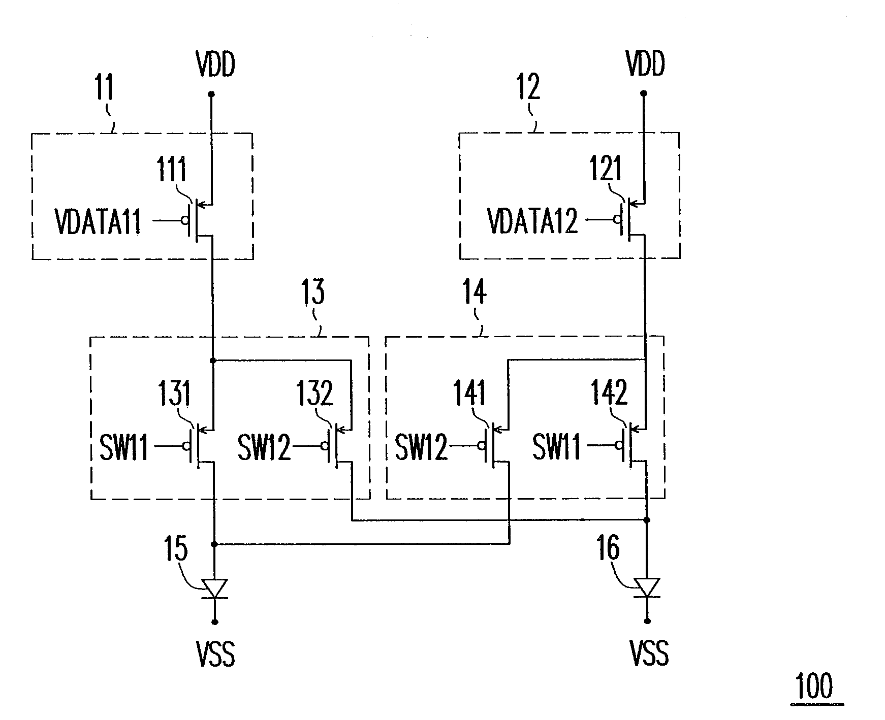
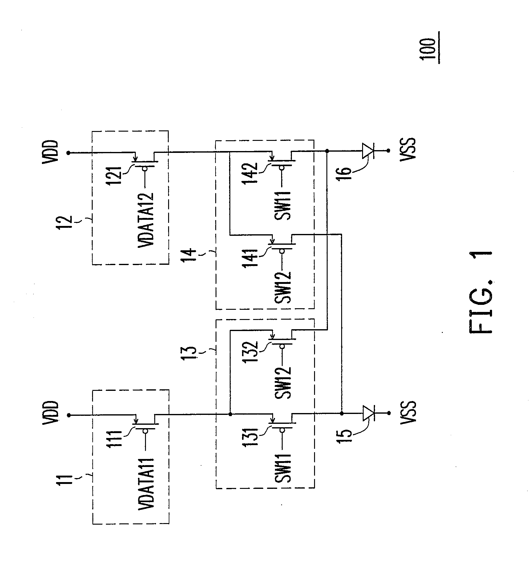
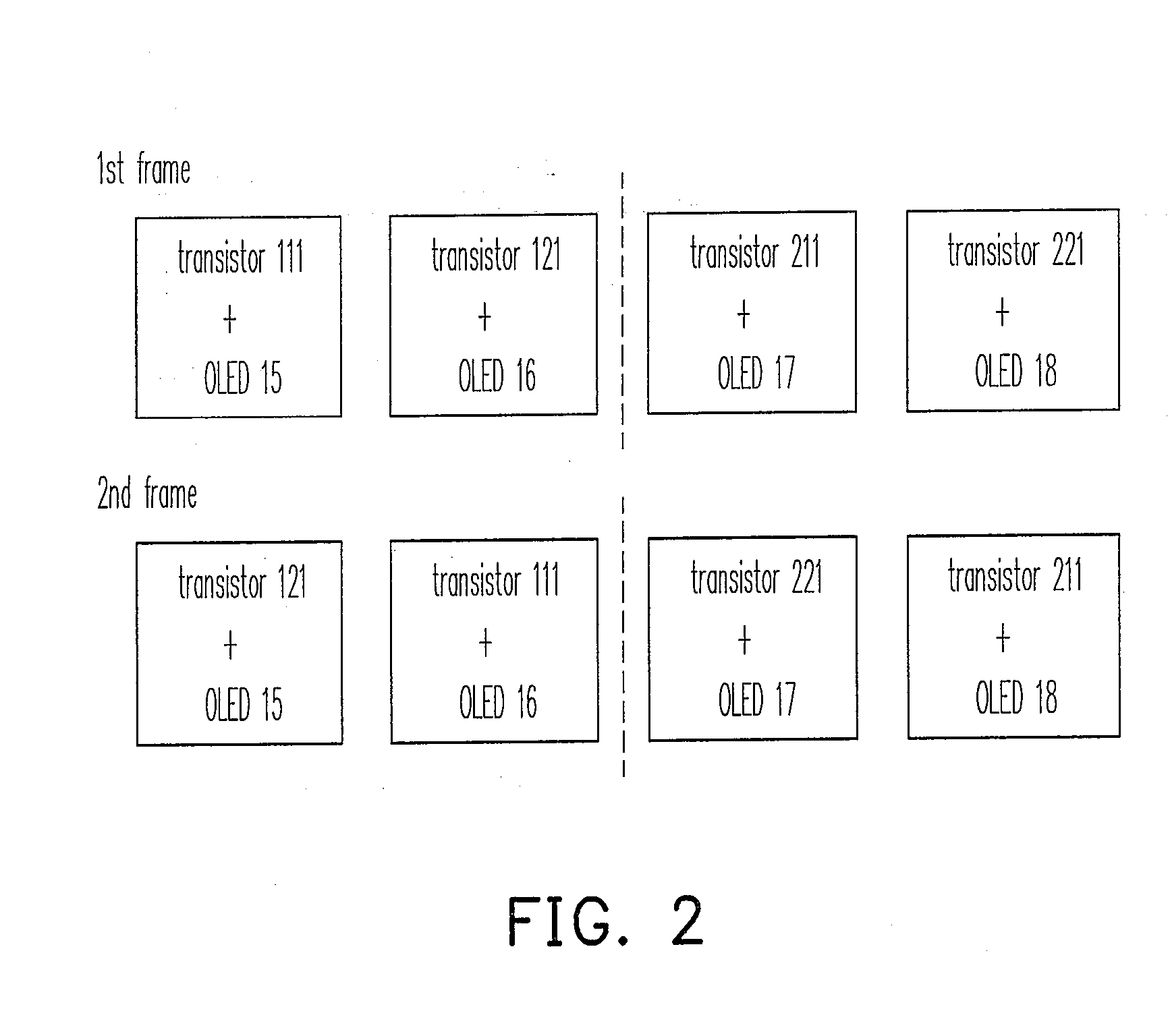
[0026]FIG. 1 is a circuit diagram of a pixel group of a pixel array according to the present invention. The pixel array is divided to a plurality of pixel groups. A pixel group 100 includes driving units 11 and 12, switching units 13 and 14, and OLEDs 15 and 16. The driving unit 11 includes a NMOS transistor 111 and the driving unit 12 includes a NMOS transistor 121. The switching unit 13 includes NMOS transistors 131 and 132 and the switching unit 14 includes NMOS transistors 141 and 142. The transistor 111 receives the data signal VDATA11 to generate and to output driving currents for the OLEDs 15 and 16. The transistor 121 receives the data signal VDATA12 to generate and to output driving currents for the OLEDs 15 and 16. The transistor 131 receives the switching signal SW11 and the transistor 132 receives the switching signal SW12. The transistor 141 receives the switching signal SW12 and the transistor 142 receives the switching signal SW11. The driving unit 11 and the driving ...
second embodiment
[0029]FIG. 3A is a circuit diagram of a pixel group of a pixel array according to the present invention. The pixel array is divided to a plurality of pixel groups. A pixel group 300A includes driving units 31 and 32, switching units 33 and 34, and OLEDs 35 and 36. The driving units 31 and 32 of the pixel group 300 are commonly connected to a scan line to receive a scan signal SCAN31. The driving unit 31 includes transistors 311 and 313 and a capacitor 312. The capacitor 312 is connected to a source of the transistor 311 and a gate of the transistor 313. The driving unit 32 includes transistors 321 and 323 and a capacitor 322. The capacitor 322 is coupled to a source of the transistor 321 and a gate of transistor 323. The switching unit 33 includes transistors 331 and 332 and the switching unit 34 includes transistors 341 and 342. The transistor 311 receives the scan signal SCAN31 and a data signal VDATA31 to generate and to output driving currents for the OLEDs 35 and 36. The transi...
third embodiment
[0030]FIG. 3B is a circuit diagram of a pixel group of a pixel array according to the present invention. A pixel group 300B includes driving units 37 and 38, switching units 33 and 34, and OLEDs 35 and 36. The driving unit 37 includes transistor 371, 373, 374, and 375 and a capacitor 372. The capacitor 372 is connected to a gate of the transistor 373 and a source of the transistor 374. The driving unit 38 includes transistors 381, 383, 384, and 385 and a capacitor 382 The transistor 371 receives a scan signal SCAN32 and a data signal VDATA31 to generate and to output driving currents for the OLEDs 35 and 36. The transistor 381 receives a scan signal SCAN32 and a data signal VDATA32 to generate and to output driving currents for the OLEDs 35 and 36. The capacitor 382 is connected to a gate of the transistor 383 and a source of the transistor 384. The switching unit 33 includes transistors 331 and 332 and the switching unit 34 includes transistors 341 and 342. The transistor 331 recei...
PUM
 Abstract
Description
Claims
Application Information
 - R&D Engineer
- R&D Manager
- IP Professional
- Industry Leading Data Capabilities
- Powerful AI technology
- Patent DNA Extraction
Browse by: Latest US Patents, China's latest patents, Technical Efficacy Thesaurus, Application Domain, Technology Topic, Popular Technical Reports.
© 2024 PatSnap. All rights reserved.Legal|Privacy policy|Modern Slavery Act Transparency Statement|Sitemap|About US| Contact US: help@patsnap.com


