Embedded inductor devices and fabrication methods thereof
- Summary
- Abstract
- Description
- Claims
- Application Information
AI Technical Summary
Benefits of technology
Problems solved by technology
Method used
Image

Examples
Embodiment Construction
[0037]The following description is of the best-contemplated mode of carrying out the invention. This description is made for the purpose of illustrating the general principles of the invention and should not be taken in a limiting sense. The scope of the invention is best determined by reference to the appended claims.
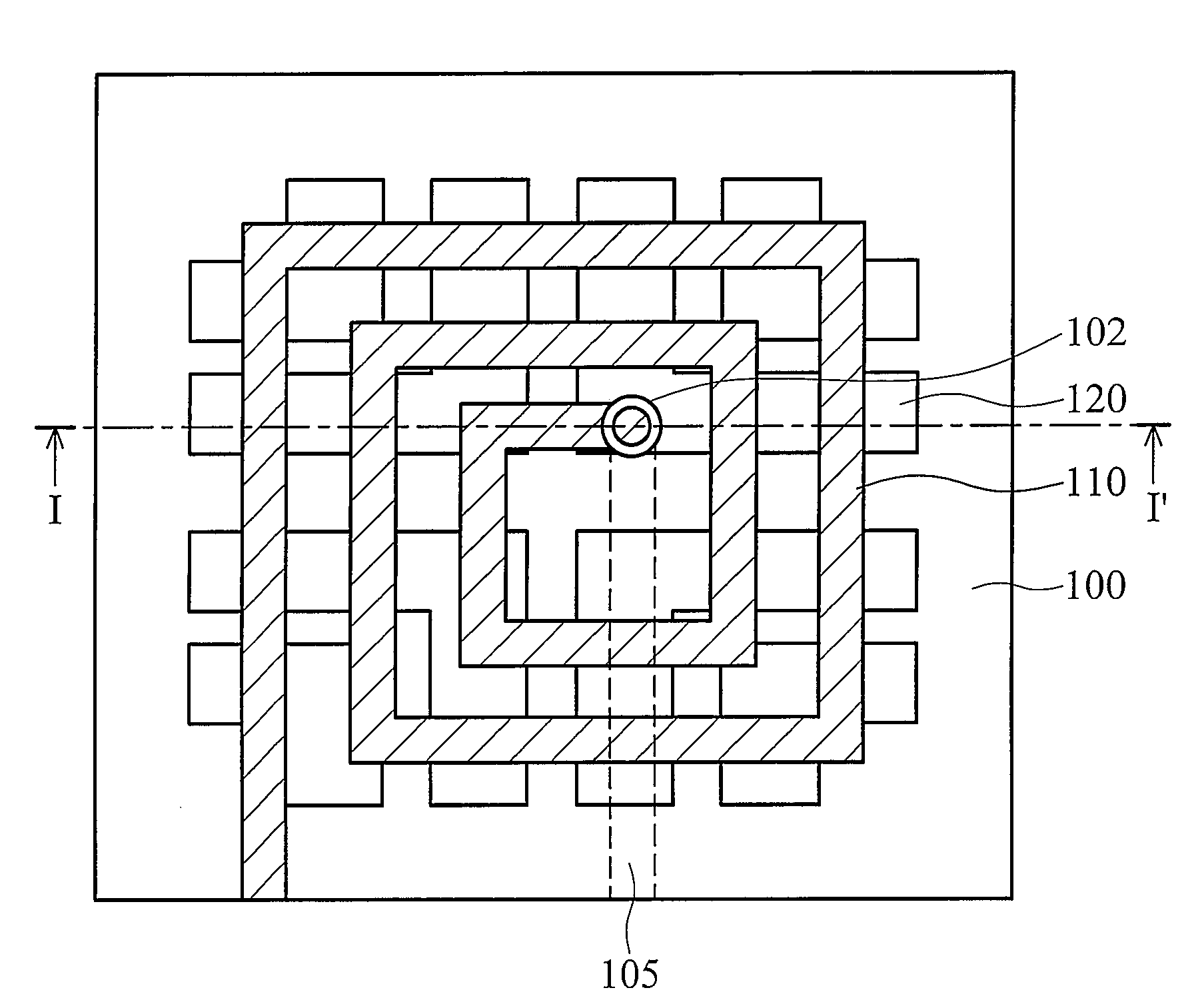
[0038]The invention is directed to applying a patterned magnetic layer with high permeability (μr>1) on an embedded inductor device to enhance inductance and quality factor as well as self-resonate frequency (SRF). More specifically, the patterned magnetic layer is substantially perpendicular to the conductive coil of the embedded inductor device at any crossover. The magnetic field generated by the conductive coil is parallel to the inducing current generated in the patterned magnetic layer to enhance the magnetic field and reducing parasitic effect and magnetic hysteresis loss. The embedded inductor device can thus maintain high inductance, high quality factor and hi...
PUM
| Property | Measurement | Unit |
|---|---|---|
| Electrical conductor | aaaaa | aaaaa |
| Permeability | aaaaa | aaaaa |
| Magnetism | aaaaa | aaaaa |
Abstract
Description
Claims
Application Information
 - R&D
- Intellectual Property
- Life Sciences
- Materials
- Tech Scout
- Unparalleled Data Quality
- Higher Quality Content
- 60% Fewer Hallucinations
Browse by: Latest US Patents, China's latest patents, Technical Efficacy Thesaurus, Application Domain, Technology Topic, Popular Technical Reports.
© 2025 PatSnap. All rights reserved.Legal|Privacy policy|Modern Slavery Act Transparency Statement|Sitemap|About US| Contact US: help@patsnap.com