Electronics device, semiconductor device, and method for manufacturing the same
a semiconductor device and electromechanical technology, applied in the direction of organic semiconductor devices, identification means, instruments, etc., can solve the problems of shortening between anodes and cathodes, and uneven surface formation of pixel electrodes, so as to prevent orientation defects of liquid crystals, eliminate unevenness, and high light transmittance
- Summary
- Abstract
- Description
- Claims
- Application Information
AI Technical Summary
Benefits of technology
Problems solved by technology
Method used
Image
Examples
embodiment 1
[0119]In this embodiment, an example of an edge portion covered with a metal layer is described with reference to FIGS. 8A and 8B. Portions other than a peripheral portion are identical with those in FIG. 2A shown in Embodiment Mode; therefore, detailed description is omitted here. Note that the same reference numerals are used in FIGS. 8A and 8B for the same parts as those in FIG. 2A.
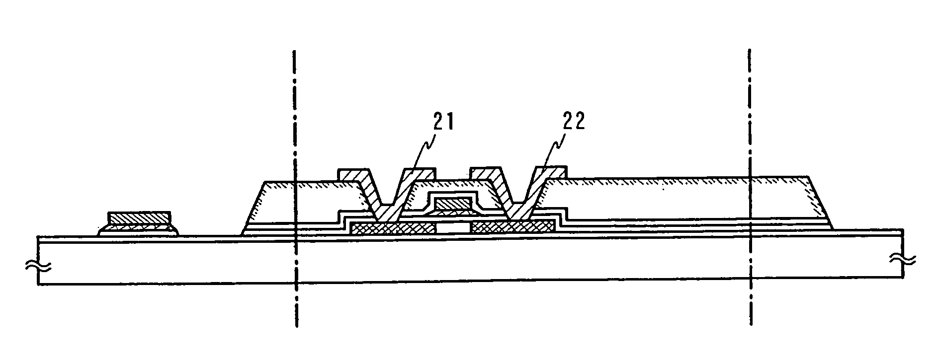
[0120]Metal layers 621 and 622 are formed by covering a circumference of a high thermostability planarizing film. The metal layers 621 and 622 may be formed simultaneously with source / drain electrodes 21 and 22, or may be separately formed by patterning. However, a part of a lead wiring to be connected to a terminal electrode is not covered with the metal layers 621 and 622, although not shown here.
[0121]FIG. 8B shows an enlarged cross-sectional view of an peripheral portion. A side surface of an edge portion having a step in the high thermostability planarizing film 16 is covered with the metal layers...
embodiment 2
[0124]In this embodiment, an example of an edge portion added with an inert element by plasma treatment is described with reference to FIG. 9. Portions other than the edge portion are identical with those in FIG. 2B shown in Embodiment Mode; therefore, detailed description is omitted here. Note that the same reference numerals are used in FIG. 9 for the same parts as those in FIG. 2B.
[0125]This embodiment is an example of forming a highly densified portion on a surface (including a side surface) by adding an inert element without forming an edge portion of a high thermostability planarizing film 16 into a tapered shape.
[0126]In this embodiment, an edge portion of the high thermostability planarizing film 16 is nearly perpendicular, and has curvature in a top edge portion thereof.
[0127]The highly densified portion can be provided on a surface (including a side surface) by a method for adding an inert element with plasma treatment even if an edge portion has such a shape as shown in F...
embodiment 3
[0130]An example of an inversely staggered TFT is described in this embodiment with reference to FIGS. 10A and 10B. Portions other than a TFT and a terminal electrode are identical with those in FIG. 2A shown in Embodiment Mode; therefore, detailed description is omitted here. Note that the same reference numerals as those in FIG. 2A are used in FIGS. 10A and 10B for the same parts as those in FIG. 2A.
[0131]A TFT shown in FIG. 10A is a channel stop type. A gate electrode 719 and a terminal electrode 715 are simultaneously formed, and a semiconductor layer containing an amorphous semiconductor film 714a, an n+ layer 718, and a metal layer 717 are laminated over a gate insulating film 12. A channel stopper 714b is formed over a portion to be a channel formation region of the semiconductor layer 714a. Further, source / drain electrodes 721 and 722 are formed.
[0132]A TFT shown in FIG. 10B is a channel etch type. A gate electrode 819 and a terminal electrode 815 are simultaneously formed, ...
PUM
| Property | Measurement | Unit |
|---|---|---|
| taper angle | aaaaa | aaaaa |
| taper angle | aaaaa | aaaaa |
| grain diameter | aaaaa | aaaaa |
Abstract
Description
Claims
Application Information
 - R&D
- Intellectual Property
- Life Sciences
- Materials
- Tech Scout
- Unparalleled Data Quality
- Higher Quality Content
- 60% Fewer Hallucinations
Browse by: Latest US Patents, China's latest patents, Technical Efficacy Thesaurus, Application Domain, Technology Topic, Popular Technical Reports.
© 2025 PatSnap. All rights reserved.Legal|Privacy policy|Modern Slavery Act Transparency Statement|Sitemap|About US| Contact US: help@patsnap.com


