Board processing apparatus and method of fabricating semiconductor apparatus

Inactive Publication Date: 2008-04-17
NTT MOBILE COMM NETWORK INC
View PDF2 Cites 187 Cited by
  • Summary
  • Abstract
  • Description
  • Claims
  • Application Information

AI Technical Summary

Benefits of technology

[0006] It is an object of the invention to provide a board processing apparatus and a method of fabricating a semiconductor apparatus for restraining a rapid flow of a gas caused by a pressure difference between a processing chamber and a preparing chamber to thereby prevent a particle from being adhered onto a board by resolving the above-described problem.
[0008] According to the invention, the second set pressure value is updated based on the pressure difference between the preparing chamber and the processing chamber detected by the pressure difference detector by the set pressure updating portion, the pressure difference between the preparing chamber and the processing chamber is reduced, and therefore, a rapid flow of a gas caused by the pressure difference is restrained to thereby enable to prevent the board from being contaminated by a particle.

Problems solved by technology

However, there poses a problem that when the load / lock chamber is once installed, it is difficult to attach and detach the load / lock chamber to and from the board processing apparatus, further, enormous labor and time is consumed in a manual wiping operation and a nonuniformity is brought about in a degree of cleaning.

Method used


Image

  • Board processing apparatus and method of fabricating semiconductor apparatus
  • Board processing apparatus and method of fabricating semiconductor apparatus
  • Board processing apparatus and method of fabricating semiconductor apparatus

Examples


example

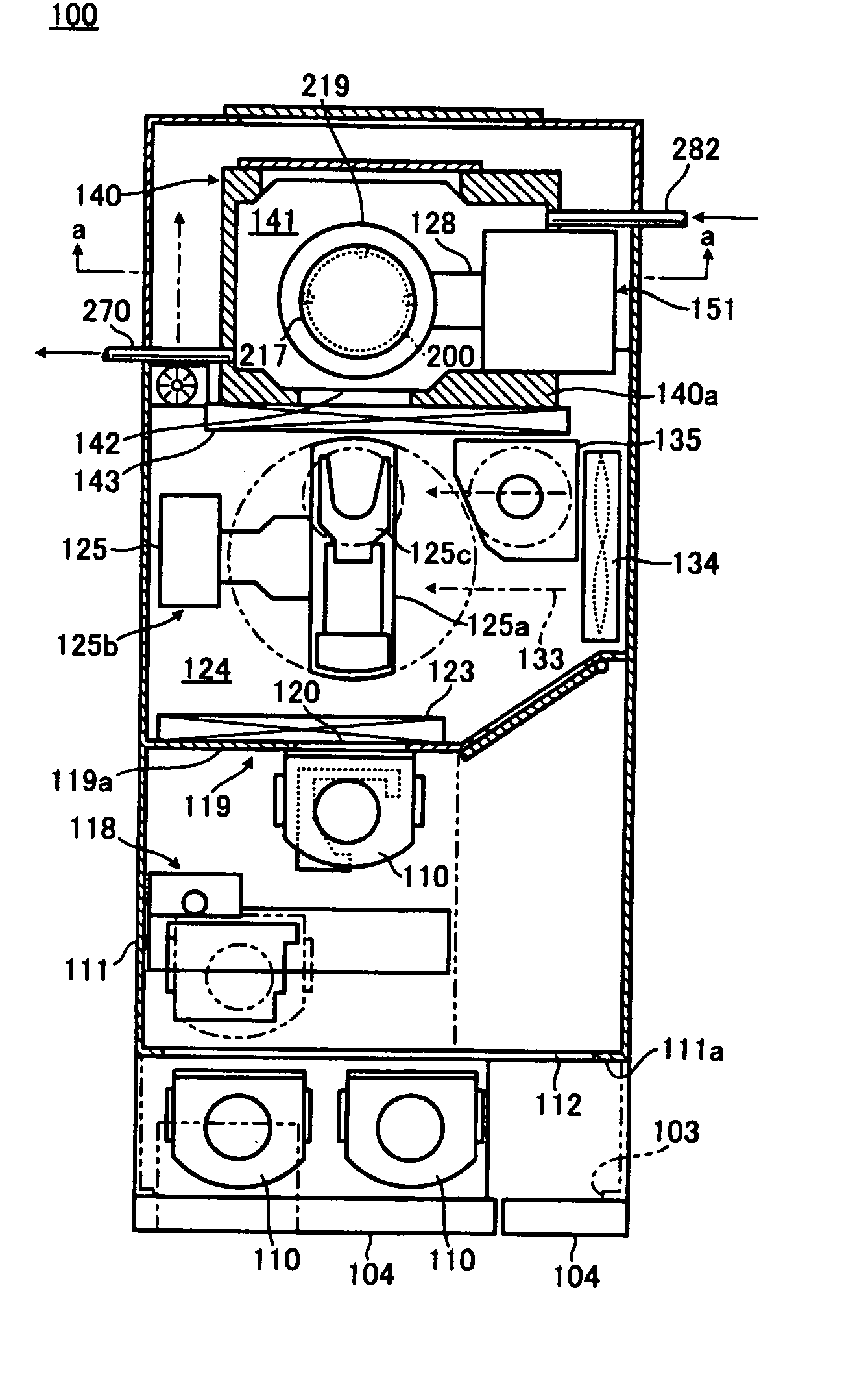
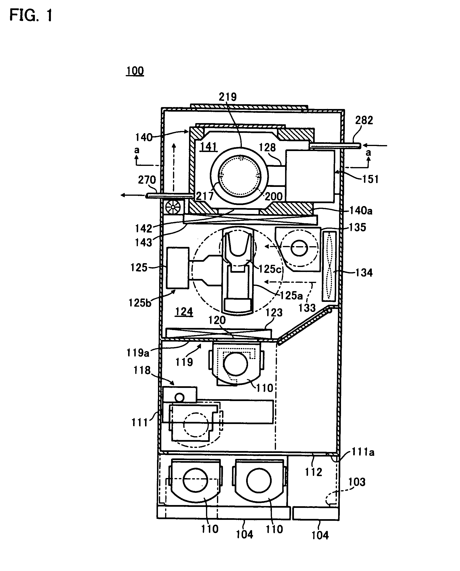
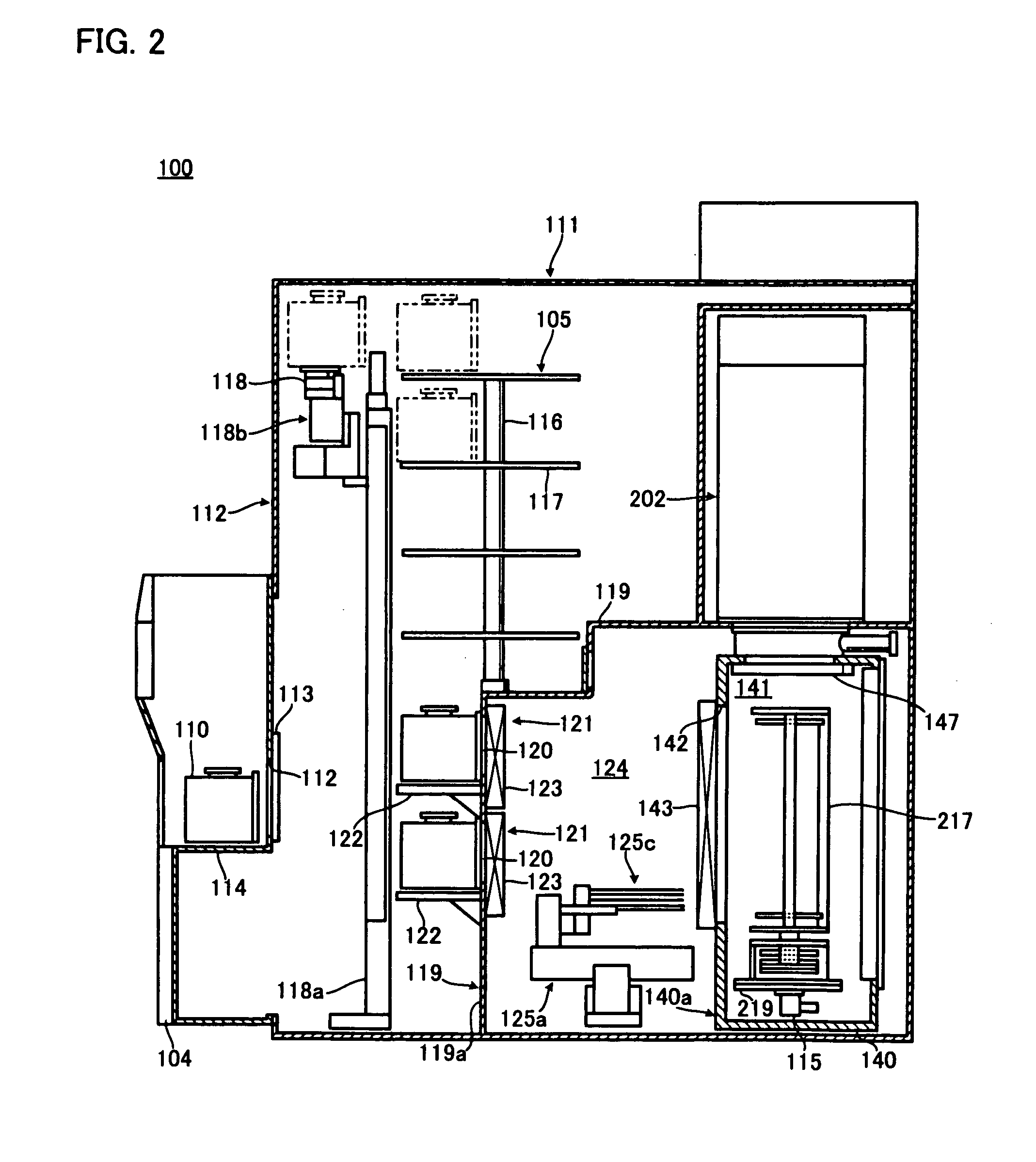
[0078] The pressure difference between the processing chamber 201 and the load / lock chamber 141 detected by the pressure difference sensor 280 is added or subtracted to or from the set pressure value on the side of the processing chamber 201 (second set pressure value), the second set pressure value is updated, and the pressure of the processing chamber 201 is regulated based on the updated set pressure value. As shown by FIG. 7B, in comparison with Comparative Examples 1 and 2, the relative pressure difference (broken line in the drawing) between the processing chamber 201 and the load / lock chamber 141 and the absolute pressure difference (difference between bold line and one-dotted chain line in the drawing) between the processing chamber 201 and the load / lock chamber 141 are reduced and the pressures of the processing chamber 201 and the load / lock chamber 141 become substantially the same.

[0079] As described above, according to the board processing apparatus 100 according to the...


PUM

PropertyMeasurementUnit
Pressureaaaaaaaaaa

Abstract

A board processing apparatus and a method of fabricating a semiconductor apparatus for reducing a pressure difference between a preparing chamber and a processing chamber and restraining a rapid flow of a gas caused by the pressure difference to thereby prevent a board from being contaminated by a particle are disclosed.

Description

BACKGROUND OF THE INVENTION [0001] 1. Field of the Invention [0002] The present invention relates to a board processing apparatus and a method of fabricating a semiconductor apparatus for processing a board of a semiconductor device or the like. [0003] 2. Description of Related Art [0004] There is known a board processing apparatus of this kind having a plurality of airtight chambers contiguous to each other of a reaction chamber (processing chamber), a load / lock chamber (preparing chamber) and the like for opening and closing intervals of the airtight chambers by closing means. For example, there is publicly known a board processing apparatus for preventing dust generation by restraining an abrupt flow of a gas caused by a pressure difference between one airtight chamber and other airtight chamber by communicating the two contiguous airtight chambers when a pressure difference between the two contiguous airtight chambers becomes equal to or lower than a predetermined value (for exa...

Claims


Application Information

Patent Timeline
IPC IPC(8): H01L21/00B05C11/00
CPCC23C16/54H01L21/67109H01L21/67775H01L21/67772H01L21/67253H01L21/02
Inventor SHIMADA, MASAKAZUTSUKAMOTO, HIDEYUKI
Owner NTT MOBILE COMM NETWORK INC
Why Eureka
Try Eureka