Eureka AIR delivers breakthrough ideas for toughest innovation challenges, trusted by R&D personnel around the world.

Double-rate memory

a memory and double-rate technology, applied in the field of memory circuits, can solve the problems of requiring costly additional space for master clocks, significant extra power, and affecting the performance of memory circuits,

Active Publication Date: 2008-02-14
NXP USA INC
View PDF5 Cites 17 Cited by
  • Summary
  • Abstract
  • Description
  • Claims
  • Application Information

AI Technical Summary

Benefits of technology

The invention is about a memory circuit that can operate at double the frequency of the system clock, without the need for an additional phase locked loop (PLL). This is achieved by using the rising and falling edges of the clock to double the rate of operation. The memory circuit uses both the rising and falling edges of the clock, making it more efficient. The invention also includes a cache memory that operates at double the frequency of the clock. The technical effect of the invention is to allow for faster operation of the memory without the need for an additional PLL.

Problems solved by technology

PLLS are relatively large circuits, and their power consumption is proportional to frequency.
Thus, the likely requirement of an additional PLL that operates at four times the master clock frequency requires costly additional space and significant extra power.

Method used


Image

  • Double-rate memory
  • Double-rate memory
  • Double-rate memory

Examples


Embodiment Construction

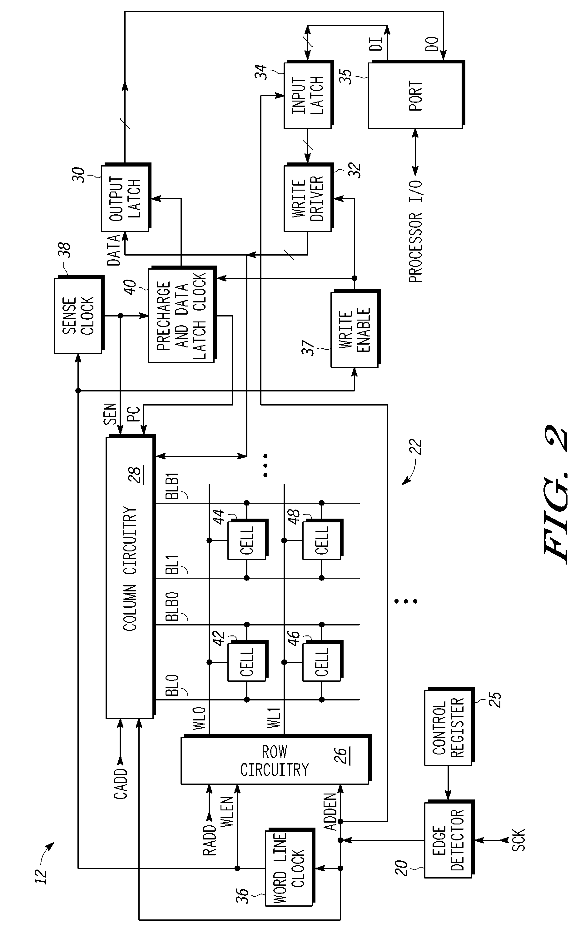
[0011]In one aspect a memory circuit uses both the rising edge and falling edge of a system clock to double the speed of operation of the memory. This is better understood by reference to the drawings and the following description.

[0012]Shown in FIG. 1 is a memory circuit 10 comprising a cache memory 12, a TAG memory 14, and an Address buffer 16. Cache memory 12 includes an edge detector 20 for receiving a clock signal. Similarly TAG memory 14 includes an edge detector 18 for receiving the clock signal. TAG memory 14 compares a portion of the address from address buffer 16 to its stored addresses to determine if there is a hit. Cache memory 12 responds to another part of the address and provides data from or writes data if it receives a hit signal from TAG memory 14. Both TAG memory 14 and cache memory 12 operate at the twice the frequency of the clock signal. Edge detectors 18 and 20 provide information as to whether the edge of the clock is a rising edge or a falling edge. An acce...


PUM


Abstract

A double-rate memory has an array of single word line memory cells arranged in rows and columns. The single word line memory cells provide and store data via a first port. Addressing and control circuitry is coupled to the array of single word line memory cells. The addressing and control circuitry receives an address enable signal to initiate an access of the array whereby an address is received, decoded, and corresponding data retrieved or stored. Edge detection circuitry receives a memory clock and provides the address enable signal upon each rising edge and each falling edge of the memory clock to perform two memory operations in a single cycle of the memory clock. A memory operation includes addressing the memory and storing data in the memory or retrieving and latching data from the memory. In another form a double-rate dual port memory permits two independent read / write memory accesses in a single memory cycle.

Description

FIELD OF THE INVENTION[0001]This invention relates to memories, and more particularly, to memory circuits that are operable at double a clock frequency.BACKGROUND OF THE INVENTION[0002]There are situations that have become more common in which a system clock is operated at a frequency well below the capability of the memory that is part of the system. The memory may even have the ability to operate at twice the frequency of the system clock. This situation can arise, for example, in the case of a cache embedded in the same integrated circuit as a processor. One technique for taking advantage of this ability of a memory is to multiply the system clock and use the multiplied clock for operating the memory. To double the frequency while keeping the clock operating properly, the master clock should not merely be doubled but quadrupled then divided by two. This will typically require an additional phase locked loop (PLL). PLLS are relatively large circuits, and their power consumption is...

Claims


Application Information

Patent Timeline
Patent Type & Authority Applications(United States)
IPC IPC(8): G11C8/00
CPCG11C7/1066G11C7/22G11C8/18G11C8/10G11C7/222
Inventor PELLEY, III, PERRY H.HOCKSTRA, GEORGE P.
Owner NXP USA INC
Why Eureka
Eureka Blog
Learn More