Test probe and manufacturing method thereof

a technology of test probes and manufacturing methods, applied in the field of test probes, can solve the problems of reducing the reliability of test, increasing the contact resistance, and difficult manufacturing, and achieves the effects of eliminating contact resistance, simple structure, and convenient manufactur

Inactive Publication Date: 2008-02-14
LEENO IND INC
View PDF6 Cites 12 Cited by
  • Summary
  • Abstract
  • Description
  • Claims
  • Application Information

AI Technical Summary

Benefits of technology

[0018]Accordingly, the present invention has been made keeping in mind the above problems occurring in the prior art, and an object of the present invention is to provide a test probe, which has a simple structure, thus affording ease of manufacture, and eliminates contact resistance during a test, thus enhancing the reliability of the test.

Problems solved by technology

However, the conventional probe is problematic in that current applied to the probe part is indirectly transmitted through the outer cylinder and the spring, so that contact resistance is increased, and thus the reliability of the test is lowered.
However, the prior art has a complicated construction, so that it is difficult to manufacture.
Further, the prior art adopts an indirect transmitting method through the outer cylinder, so that contact resistance may be increased or the elastic force of the spring may be lost due to over-current.
Further, since current applied to the probe part of the probe is transmitted through the outer cylinder and the spring to the PCB, the signal path is lengthened, so that the reliability of the test is poor.

Method used


Image

  • Test probe and manufacturing method thereof
  • Test probe and manufacturing method thereof
  • Test probe and manufacturing method thereof

Examples


Embodiment Construction

[0037]Reference now should be made to the drawings, in which the same reference numerals are used throughout the different drawings to designate the same or similar components.

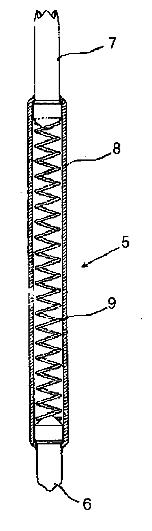
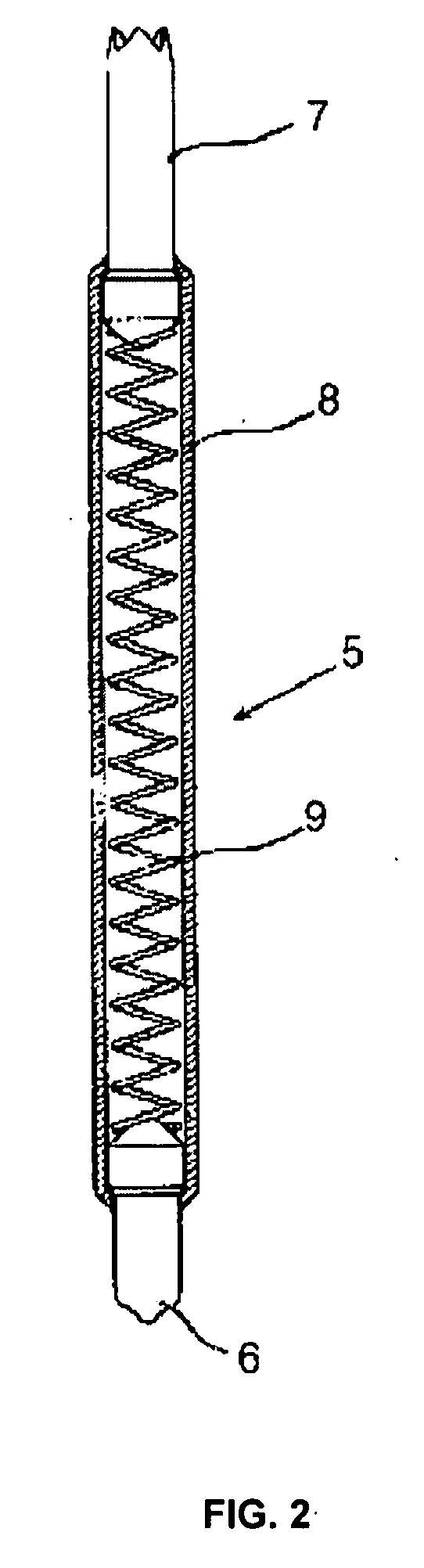
[0038]FIGS. 3a and 3b are front views showing a test probe, according to the preferred embodiment of the present invention.

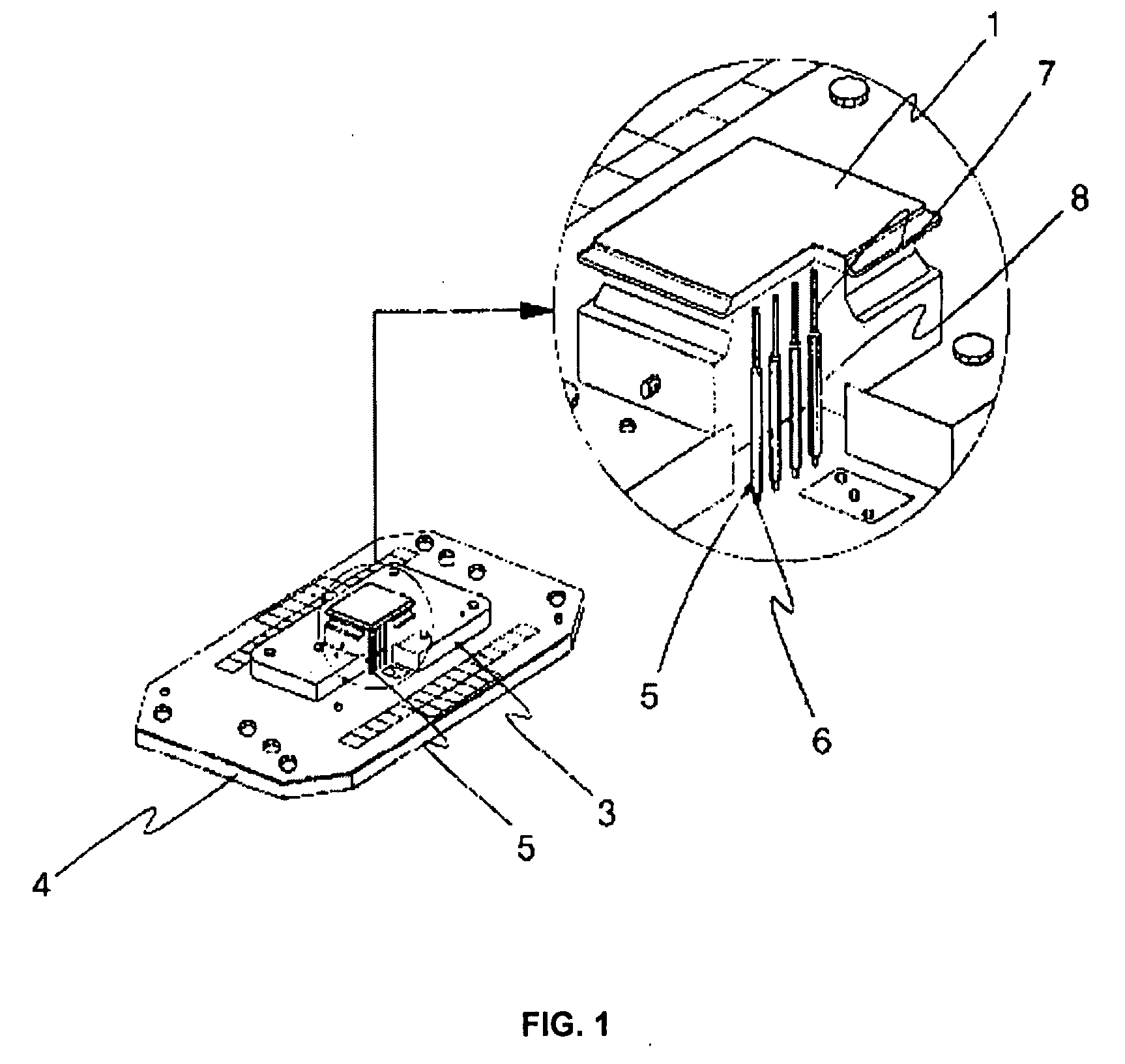
[0039]As shown in the drawings, the test probe of the present invention has on the upper portion thereof a probe part 100 which contacts a contact terminal of an object to be tested. A spring part 200, providing elastic force, extends integrally from the lower portion of the probe part 100.

[0040]According to the present invention, the probe part 100 is integrated with the spring part 200, unlike the conventional probe. Thus, when current for a test flows, the current is transmitted directly from a microchip through the probe part 100 to the spring part 200 for testing of the microchip using a contact pin connected to the lower end of the probe. Therefore, the contact resistance of the prob...


PUM

PropertyMeasurementUnit
elastic forceaaaaaaaaaa
lead angleaaaaaaaaaa
conical shapeaaaaaaaaaa

Abstract

Disclosed herein are a test probe and a method of manufacturing the test probe. The invention has a simple structure, thus affording ease of manufacture, and eliminates contact resistance during a test, thus enhancing the reliability of the test. The test probe includes a probe part which is provided on the upper portion of the probe and contacts a contact terminal of an object to be tested. A spring part, providing elastic force, extends integrally from the lower portion of the probe part, so that current flows from the object to the lower portion of the spring part. According to this invention, the spring part is integrally provided on the lower portion of the probe part, thus having a simple structure and affording ease of manufacture, and measuring current is transmitted directly from the probe part to the spring part, thus eliminating contact resistance and shortening the signal path, therefore enhancing the reliability of a test.

Description

FIELD OF THE INVENTION[0001]The present invention relates generally to a test probe and a method of manufacturing the test probe and, more particularly, to a test probe and a method of manufacturing the test probe, in which a spring part providing elastic force extends integrally from the lower portion of a probe part contacting a contact terminal of an object to be tested.BACKGROUND OF THE INVENTION[0002]Generally, a plurality of chips is installed in various kinds of electronic products. The chips play an important role in determining the performance of the electronic products.[0003]The chips are integrated circuits which carry out various functions using the logic elements formed on thin and small wafers. Each chip conducts its function in response to an electric signal which is transmitted from a printed circuit board (PCB) through a bus to the chip.[0004]The PCB comprises a thin substrate made of an insulator, such as epoxy or bakelite resin. Circuit wiring is formed on the sub...

Claims


Application Information

Patent Timeline
Patent Type & Authority Applications(United States)
IPC IPC(8): G01R1/067H01R43/00
CPCG01R1/06722G01R3/00Y10T29/49117H01R43/16H01R2201/20H01R13/2421
Inventor LEE, CHAE YOON
Owner LEENO IND INC
Why Eureka
Try Eureka