Electro-optic device substrate, electro-optic device, electronic apparatus and method for manufacturing electro-optic device substrate
- Summary
- Abstract
- Description
- Claims
- Application Information
AI Technical Summary
Benefits of technology
Problems solved by technology
Method used
Image
Examples
first embodiment
A: TFT Substrate and Liquid Crystal Display Device
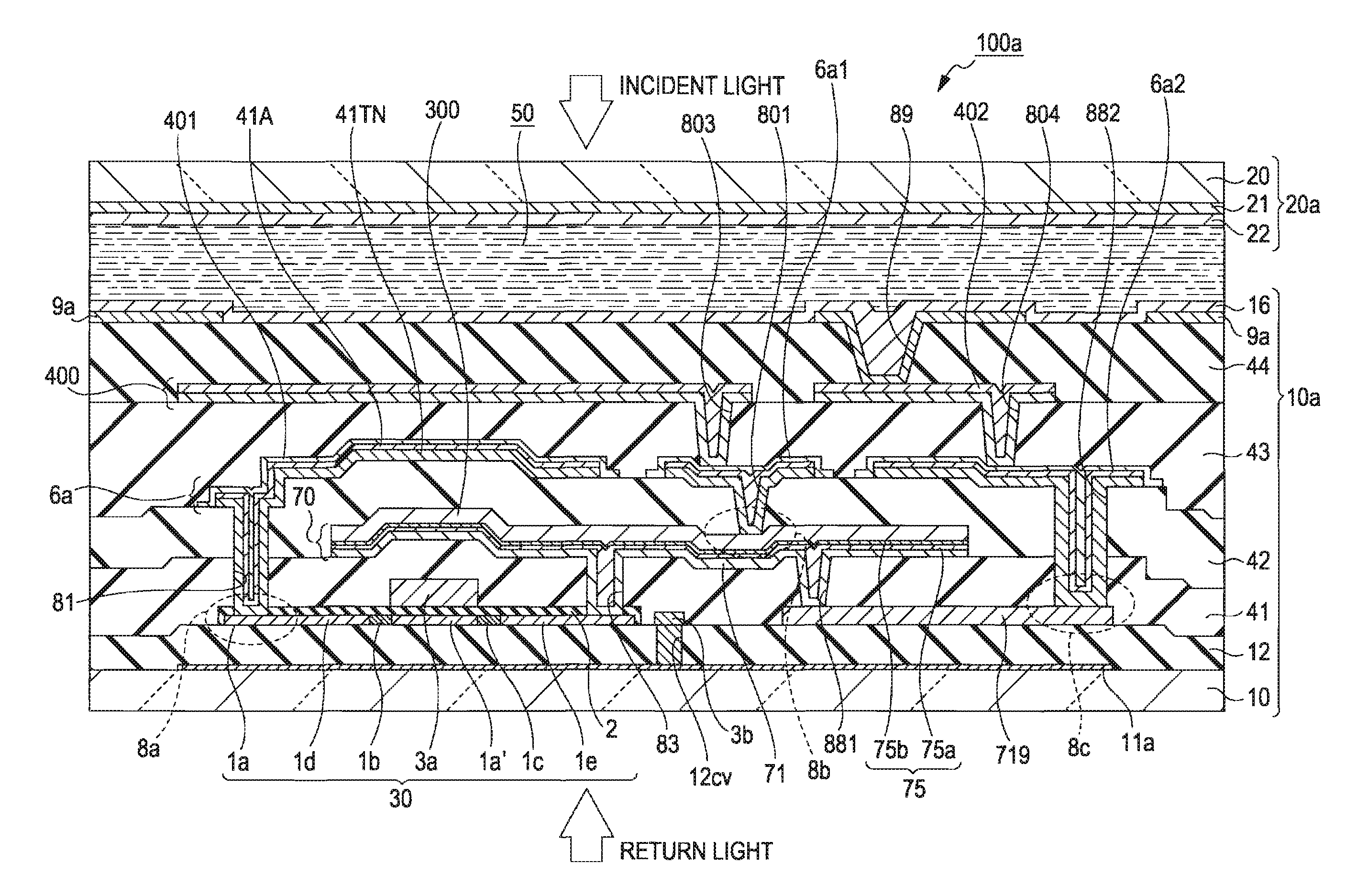
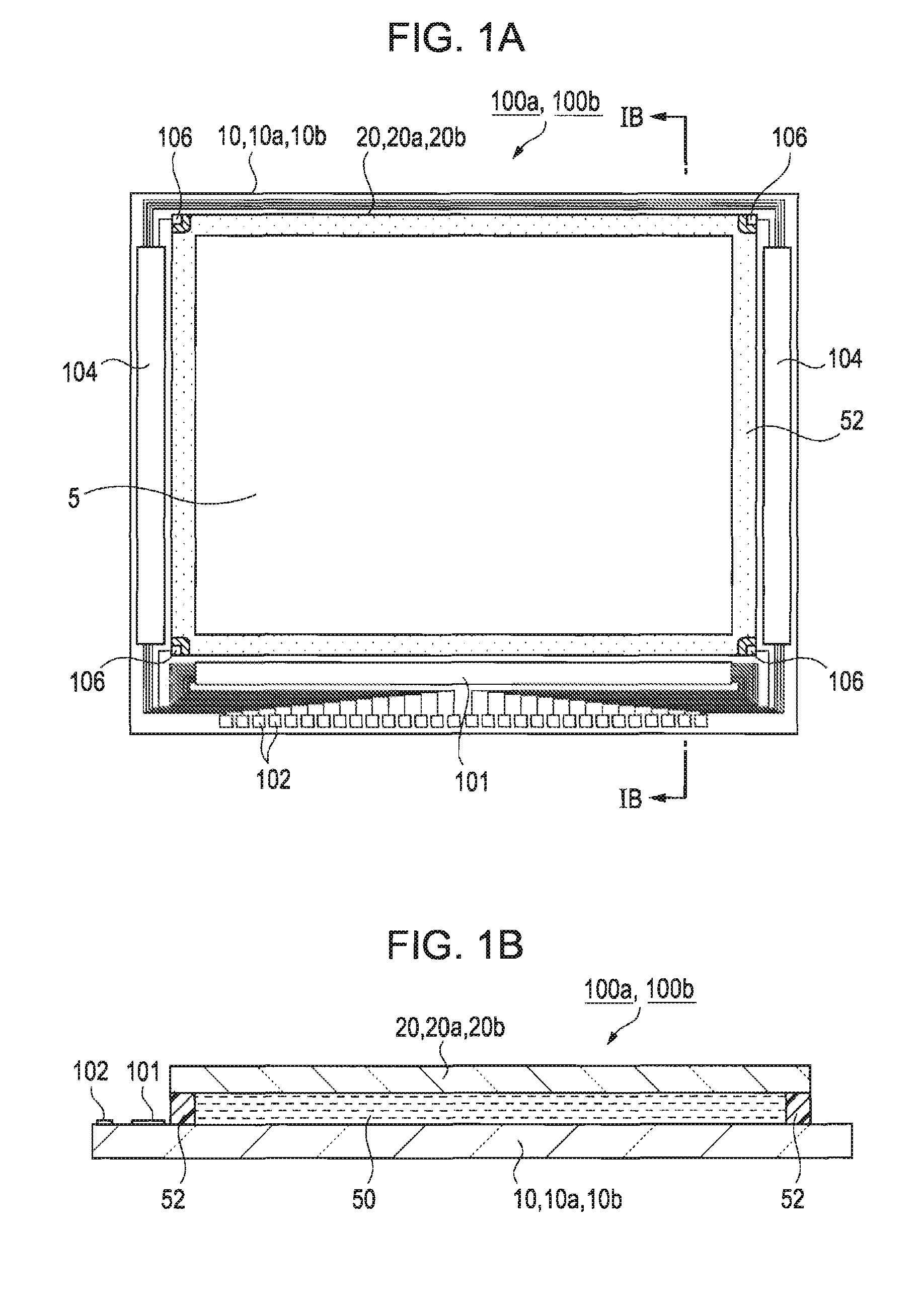
[0041]FIG. 1A is a plan view of a liquid crystal display device 100a according to a first embodiment of the invention and FIG. 1B is a sectional view taken along line IB-IB of FIG. 1A.
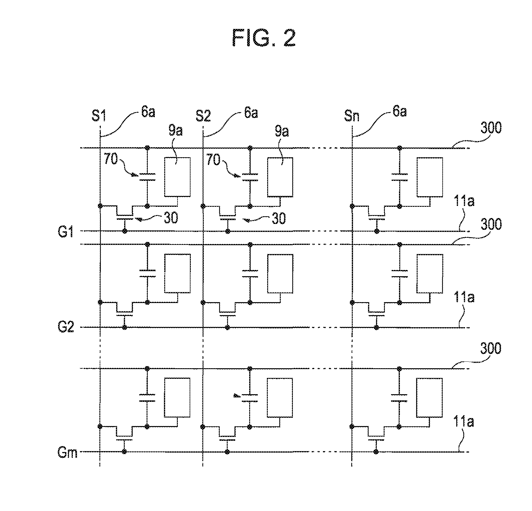
[0042]The liquid crystal display device 190a, which is an embodiment of an electro-optic device of the invention, includes a TFT substrate 19a including, for example, a quartz or glass base 10 and an opposing substrate 20a including, for example, a quartz or glass base 20. The TFT substrate 10a corresponds to an electro-optic device substrate of the invention. The TFT substrate 10a and the opposing substrate 20a are bonded together with a frame-like sealant 52 therebetween, and the space surrounded by the sealant 52 between the two substrates is defined as an image display region 5. The image display region 5 is filled with liquid crystal, to form a liquid crystal layer 50. The liquid crystal corresponds to an electrooptic material of the invention. A d...
second embodiment
[0110]A second embodiment of the invention will now be described in which a liquid crystal display device 100b has a different structure from that of the first embodiment. The liquid crystal display device 100b of the present embodiment has a multilayer structure partially different from that of the liquid crystal display device 100a according to the first embodiment. The following description does not illustrate the same components as in the liquid crystal display device 100a of the first embodiment.
[0111]The plan view and sectional view of the liquid crystal display device 100b is shown in FIGS. 1A and 1B. FIG. 12 is a sectional view of the detailed pixel structure of the liquid crystal display device 100b. In this figure, the TFT substrate 10b including the base 10 to the pixel electrode 9a corresponds to an electro-optic device substrate of the invention.
[0112]A first layer on, for example, a glass or quartz base 10 includes scanning lines 11a. A base insulating layer 12 is form...
modification 1
[0128]When the contact hole 81 is formed in the second insulating interlayer 42, the contact hole 81 may pass through the heavily doped source region 1d of the TFT element 30 (corresponding to the silicon layer in the invention) depending on the variation of etching rate (FIG. 13A). In this instance, the metal wire (for example, the data line 6a) in the contact hole 81 comes into contact with the heavily doped source region 1d at a section of the heavily doped source region 1d. In such a case, the contact area is generally short and the contact resistance is accordingly increased. The invention can prevent such a problem.
[0129]Specifically, a titanium layer 41a and a titanium nitride layer 41b are formed in the contact hole 81 passing through the heavily doped source region 1d (FIG. 13A) in the same manner as in the above-described embodiments (FIG. 13B), followed by annealing. Thus the portion in contact with the titanium layer 41a at a section of the heavily doped source region1d,...
PUM
 Abstract
Description
Claims
Application Information
 - R&D
- Intellectual Property
- Life Sciences
- Materials
- Tech Scout
- Unparalleled Data Quality
- Higher Quality Content
- 60% Fewer Hallucinations
Browse by: Latest US Patents, China's latest patents, Technical Efficacy Thesaurus, Application Domain, Technology Topic, Popular Technical Reports.
© 2025 PatSnap. All rights reserved.Legal|Privacy policy|Modern Slavery Act Transparency Statement|Sitemap|About US| Contact US: help@patsnap.com


