Complementary signal generating circuit
a signal generation circuit and signal technology, applied in logic circuits, logic circuit coupling/interface arrangements, pulse techniques, etc., can solve the problems of large influence of production tolerance, large difference in delay or difference in delay between in-phase signal and reverse phase signal, etc., to suppress the influence of production tolerance and reduce delay differences.
- Summary
- Abstract
- Description
- Claims
- Application Information
AI Technical Summary
Benefits of technology
Problems solved by technology
Method used
Image

Examples
first embodiment
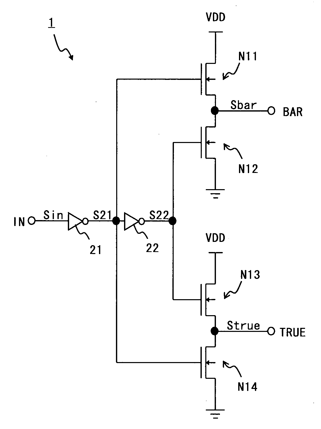
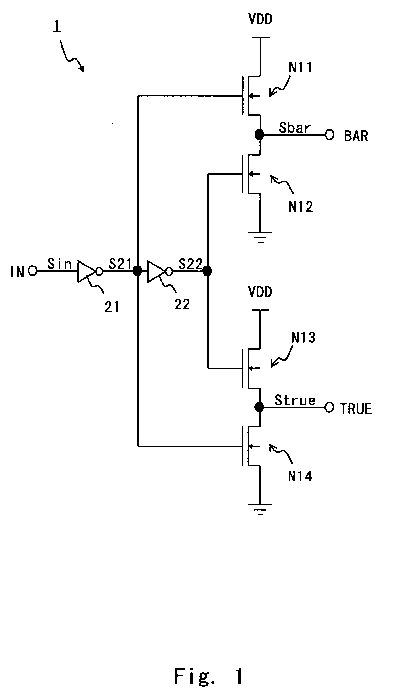
[0037]First, a complementary signal generating circuit according to a first embodiment of the present invention is described. In the complementary signal generating circuit of this embodiment, an in-phase signal output stage including two transistors has a same circuit configuration with a reverse phase signal output stage including two transistors.
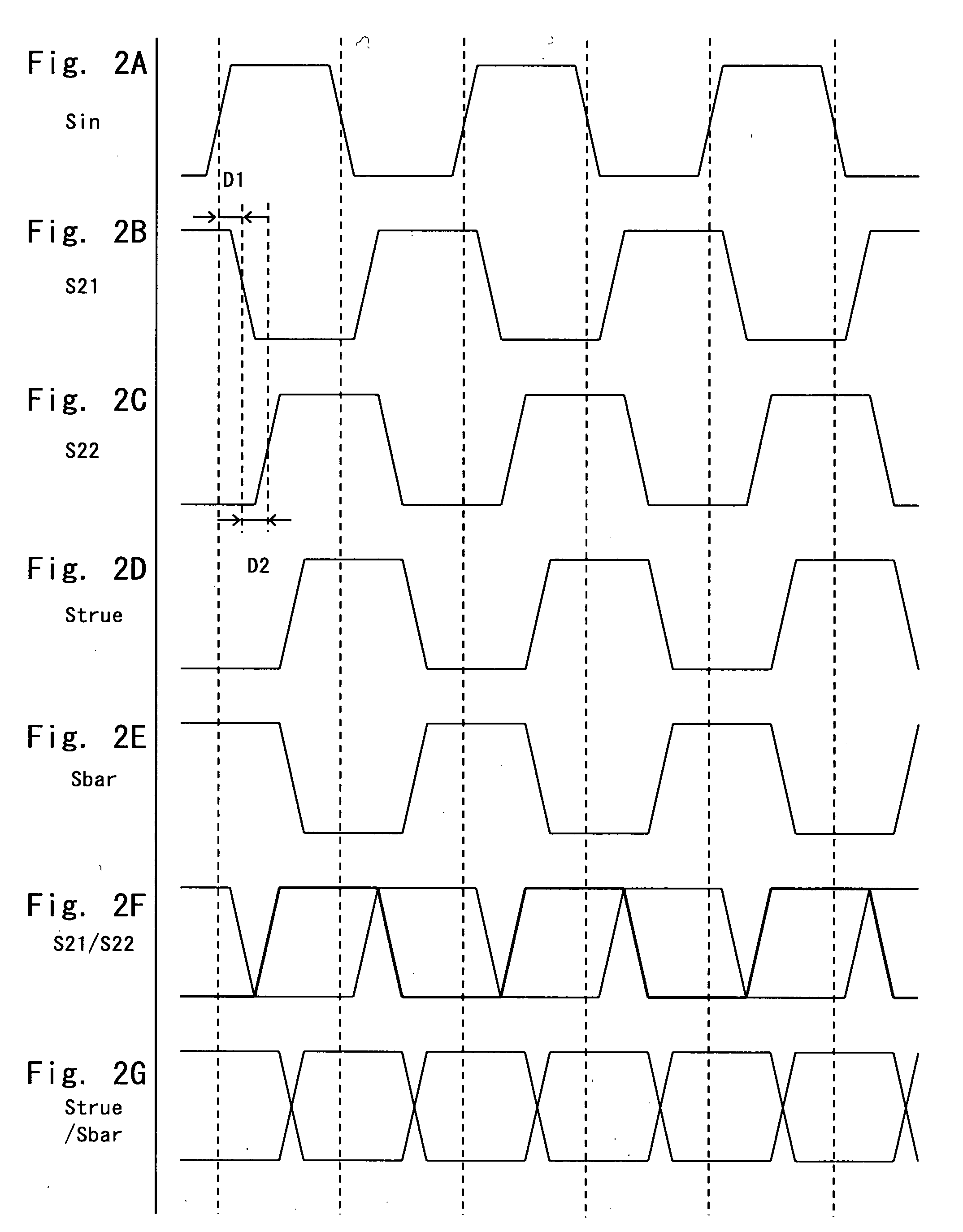
[0038]Referring to a circuit diagram of FIG. 1, the configuration of the complementary signal generating circuit of this embodiment is described. In a complementary signal generating circuit 1, if an input signal Sin such as a clock signal is input to an input terminal IN, an in-phase signal Strue that is in phase with the input signal is output from a terminal TRUE, and a reverse phase signal Sbar that is opposite in phase to the input signal is output from a terminal BAR.
[0039]As shown in FIG. 1, the complementary signal generating circuit 1 includes N-channel MOS transistors N11, N12, N13, and N14 and inverters 21 and 22. The inverters...
second embodiment
[0066]Next, a correction signal generating circuit according to a second embodiment of the present invention is described. In this embodiment, other devices are used in place of the N-channel MOS transistors of the first embodiment.
[0067]FIG. 4 is a circuit diagram of the configuration of the complementary signal generating circuit of this embodiment. The N-channel MOS transistors N11 and N13 of FIG. 1 are replaced with transfer gates G11 and G13. Further, an inverter 23 is added. In FIG. 4, the same components as those of FIG. 1 are denoted by identical reference numerals.
[0068]The inverter 23 is connected with the inverters 21 and 22 in series. The inverter 23 inverts the in-phase signal S22 from the inverter 22 to generate a reverse phase signal S23 (third signal).
[0069]The transfer gate G11 (first transfer gate) is composed of an N-channel MOS transistor (first transistor) and a P-channel MOS transistor (fifth transistor) which are connected in parallel. The transfer gate G13 (s...
third embodiment
[0082]Next, a signal generating circuit according to a third embodiment of the present invention is described. In the signal generating circuit of this embodiment, a level shifting circuit is connected with the complementary signal generating circuit of the second embodiment.
[0083]FIG. 7 is a circuit diagram of the configuration of the signal generating circuit of this embodiment. In this signal generating circuit, the complementary signal generating circuit 1 of FIG. 4 is connected with a level shifting circuit 30 of FIG. 11. The in-phase signal Strue of the complementary signal generating circuit 1 is supplied to gates of the P-channel MOS transistor P102 and the N-channel MOS transistor N101. The reverse phase signal Sbar of the complementary signal generating circuit 1 is supplied to gates of the P-channel MOS transistor P104 and the N-channel MOS transistor N102. Each circuit configuration is the same as those of FIGS. 4 and 11.
[0084]In a conventional complementary signal gener...
PUM
 Abstract
Description
Claims
Application Information
 - R&D
- Intellectual Property
- Life Sciences
- Materials
- Tech Scout
- Unparalleled Data Quality
- Higher Quality Content
- 60% Fewer Hallucinations
Browse by: Latest US Patents, China's latest patents, Technical Efficacy Thesaurus, Application Domain, Technology Topic, Popular Technical Reports.
© 2025 PatSnap. All rights reserved.Legal|Privacy policy|Modern Slavery Act Transparency Statement|Sitemap|About US| Contact US: help@patsnap.com