Semiconductor device and method for producing the same

a semiconductor and inverter technology, applied in semiconductor devices, solid-state devices, instruments, etc., can solve the problems of reducing the leakage current between the conductive region constituting the local data line and the well, reducing the reading performance, and reducing the writing performance, so as to reduce the junction leakage current, and improve the punch-through endurance of the problem.

Inactive Publication Date: 2007-09-06
RENESAS TECH CORP
View PDF3 Cites 4 Cited by
  • Summary
  • Abstract
  • Description
  • Claims
  • Application Information

AI Technical Summary

Benefits of technology

[0015] On the other hand, in the cell method (Patent Document 2) using the inversion layer as the data line, it is not required to form a diffusion layer with the result that it becomes possible to decrease the junction leakage current of the problem (2) and to improve the punch-through endurance of the problem (3) as compared with the case in which the diffusion layer is used. However, in the generation of the 50 nm design rule, there arises a problem in that the resistance of the data line using the inversion layer rapidly increases and particularly, the reading performance is lowered

Problems solved by technology

There are required three problems to be solved in a flash memory which has so-called contact-less type memory array configuration in which a source and drain of a memory cell transistor is used as a local data line, namely, the data line is formed under the word line so that there is no contact holes for data line in each memory cell, as problems arise in scaling.
There arises a problem in that when the electric resistance of the data line is heightened, the reading performance is part

Method used


Image

  • Semiconductor device and method for producing the same
  • Semiconductor device and method for producing the same
  • Semiconductor device and method for producing the same

Examples


first embodiment

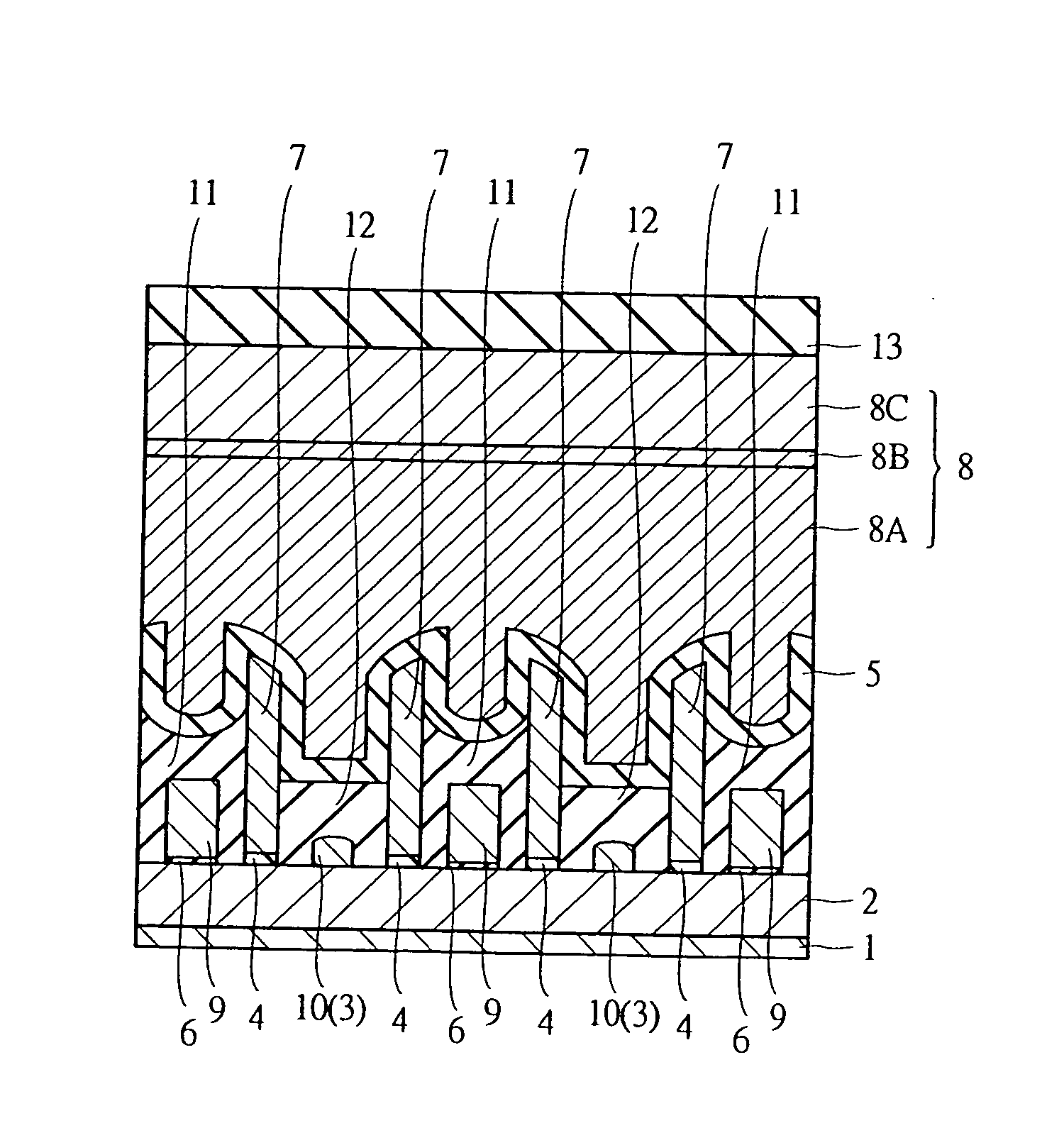
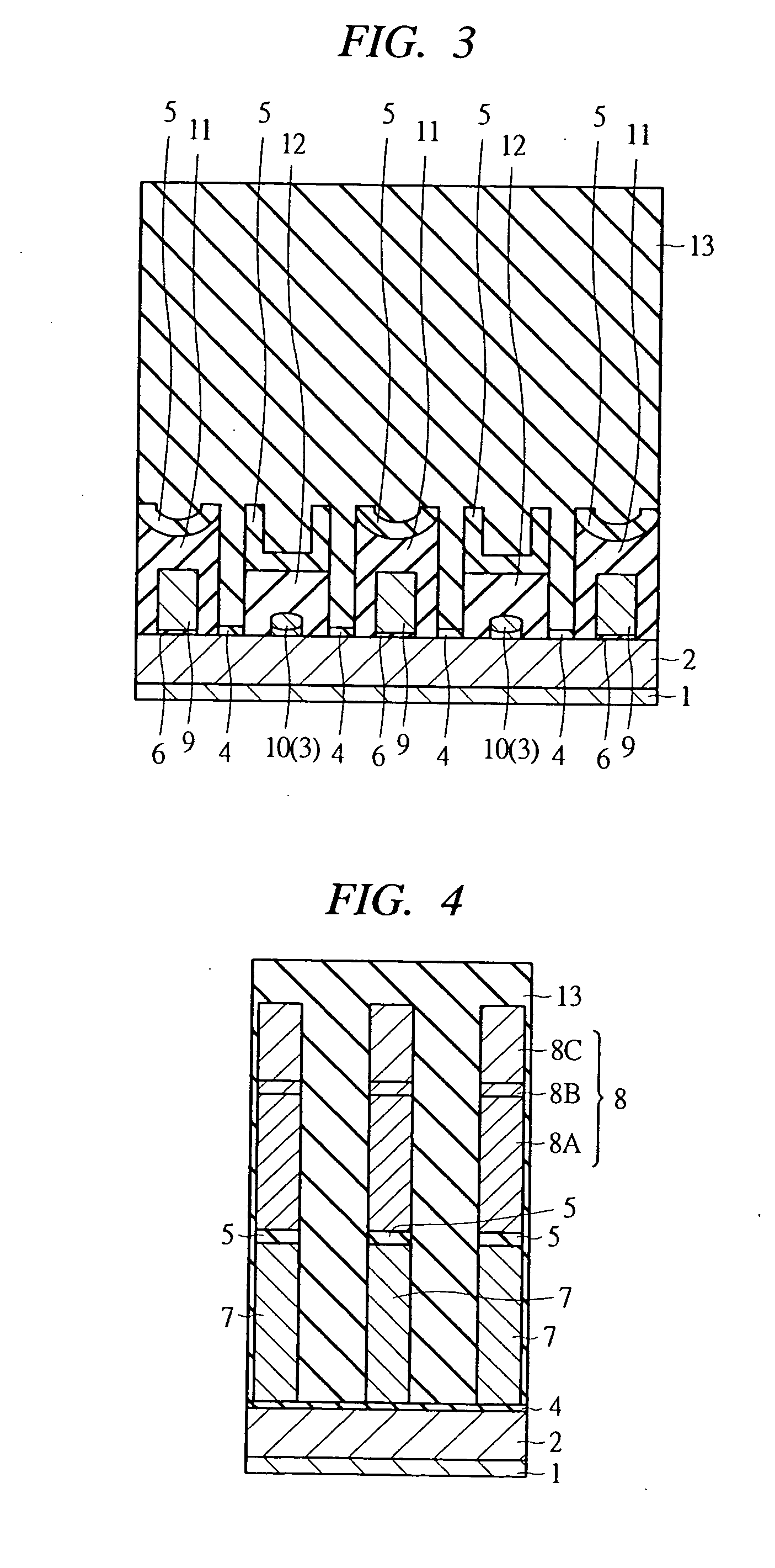
[0077]FIG. 1 through FIG. 6 show a memory array of a semiconductor memory device according to a first embodiment of the present invention. FIG. 1 is a plan view of a main part showing a memory array structure. FIG. 2 is a sectional view of a main part of a semiconductor substrate taken along line A-A′ of FIG. 1. FIG. 3 is a sectional view of a main part of the semiconductor substrate taken along line B-B′ of FIG. 1. FIG. 4 is a sectional view of a main part of the semiconductor substrate taken along line C-C′ of FIG. 1. FIG. 5 is a sectional view of a main part of the semiconductor substrate taken along line D-D′ of FIG. 1. FIG. 6 is a sectional view of a main part of the semiconductor substrate taken along line E-E′ of FIG. 1. In FIG. 1 (the plan view), for the sake of facilitating the visualization of FIG. 1, a part of members such as an insulation layer is omitted in the drawing.

[0078] The semiconductor memory device according to the first embodiment is a so-called flash memory ...

embodiment 2

[0114]FIGS. 28 through 31 show a memory array of a semiconductor memory device according to a second embodiment of the present invention. FIG. 28 is a plan view of a main part of a memory array structure. FIG. 29 is a sectional view of a semiconductor substrate taken along line A-A′ of FIG. 28. FIG. 30 is a sectional view of a main part of the semiconductor substrate taken along line B-B′ of FIG. 28. FIG. 31 is a sectional view of a main part of the semiconductor substrate taken along line C-C′ of FIG. 28. Incidentally, in FIG. 28 (a plan view), for the sake of facilitating the visualization of the drawings, a part of the members such as an insulation layer is omitted.

[0115] In the first embodiment, the assist gate 9 is formed, and the inversion layer which is formed by applying a positive voltage to the assist gate 9 is also used as a local data line. The second embodiment is different from the first embodiment in that, as shown in FIG. 28 through 31, the laminated semiconductor l...

embodiment 3

[0127]FIGS. 35 through 38 show a memory array of a semiconductor memory device according to a third embodiment of the present invention. FIG. 35 is a plan view of a main part of a memory array structure. FIG. 36 is a sectional view of a main part of a semiconductor substrate taken along line A-A′ of FIG. 35. FIG. 37 is a sectional view of a main part of the semiconductor substrate taken along line B-B′ of FIG. 35. FIG. 38 is a sectional view of a main part of the semiconductor substrate taken along line C-C′ of FIG. 35.

[0128] In the first and second embodiments, the floating gate is used as the charge accumulation layer of the memory cell transistor. However, in the third embodiment, as shown in FIGS. 35 through 38, the structure thereof is different in that the structure of the memory cell transistor is formed as a so-called MONOS type structure. Though not shown in the drawings, MNOS-type / MNS-type can be also adopted similarly.

[0129] The semiconductor memory device according to ...


PUM


Abstract

A semiconductor device comprises a floating gate which is formed on a semiconductor substrate of a first conductive type interposing a first gate insulation layer therebetween, a second charge retaining area which is formed on the semiconductor substrate interposing a second insulation layer, a control gate which is formed on the floating gate interposing a second gate insulation layer therebetween, a second gate electrode which extends in the first direction and which is formed on the second charge retaining region interposing the second gate insulation layer therebetween, and a semiconductor layer which extends in a second direction and which is formed on the semiconductor substrate so as to intersect the first and the second gate electrode are provided; wherein an n-type conductive region of a second conductive type is formed on the semiconductor layer. Consequently, it achieves high-integration of a semiconductor device.

Description

CROSS-REFERENCE TO RELATED APPLICATION [0001] The present application claims priority from Japanese Patent Application No. JP 2006-002428 filed on Jan. 10, 2006, the content of which is hereby incorporated by reference into this application. TECHNICAL FIELD OF THE INVENTION [0002] The present invention relates to a semiconductor device, and a method for producing the same. In particular, the invention relates to a technology effectively applied to higher integration and higher performance of an electrically rewritable non-volatile semiconductor memory device. BACKGROUND OF THE INVENTION [0003] So-called flash memory is known among electrically rewritable non-volatile semiconductor memory devices, as a memory in which information can be erased in block. Flash memory is excellent in portability and anti-shock properties, and also allows electrical erase of information in block. Consequently, a demand on flash memory is rapidly expanding in recent years as a memory device for use in sm...

Claims


Application Information

Patent Timeline
IPC IPC(8): H01L29/80
CPCG11C16/0433H01L27/115H01L27/11521H01L29/792H01L29/42344H01L29/7881H01L29/42328H10B69/00H10B41/30
Inventor ISHIGAKI, TAKASHIOSABE, TAROKOBAYASHI, TAKASHIIMAISHIMIZU, MASAHIRO
Owner RENESAS TECH CORP
Why Eureka
Try Eureka