Split gate type non-volatile memory device and method of manufacturing the same
- Summary
- Abstract
- Description
- Claims
- Application Information
AI Technical Summary
Benefits of technology
Problems solved by technology
Method used
Image

Examples
Embodiment Construction
[0019] Preferred embodiments of a NOR-type non-volatile memory device of a split gate structure according to the present invention and a method manufacturing the same will be described with reference to the attached drawings.
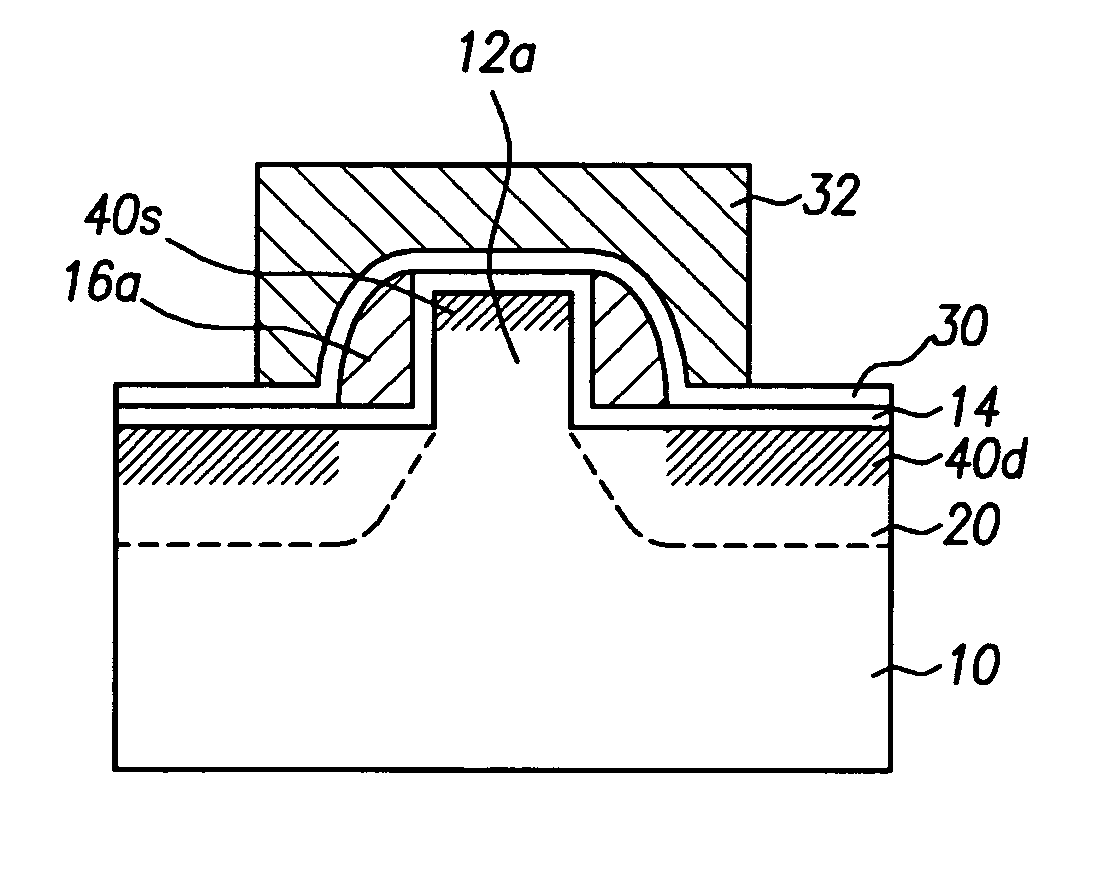
[0020] Referring to FIG. 2A, a protrusion 12 of predetermined height is formed on a silicon substrate 10. The protrusion 12 can be formed by etching the substrate 10. The protrusion 12 is extended in the direction of a word line. Then, a plurality of device isolation layer 20 that define an active region are formed on both sides of the protrusion 12. The device isolation layer 20 is formed in a field region adjacent to the active region (refer to FIG. 3).
[0021] On the other hand, the device isolation layer 20 is preferably formed after forming the protrusion 12 on the substrate through a common device isolation layer process such as shallow trench isolation (STI) process. The, device isolation layer 20 is divided on both sides due to the protrusion 12. When th...
PUM
 Abstract
Description
Claims
Application Information
 - R&D
- Intellectual Property
- Life Sciences
- Materials
- Tech Scout
- Unparalleled Data Quality
- Higher Quality Content
- 60% Fewer Hallucinations
Browse by: Latest US Patents, China's latest patents, Technical Efficacy Thesaurus, Application Domain, Technology Topic, Popular Technical Reports.
© 2025 PatSnap. All rights reserved.Legal|Privacy policy|Modern Slavery Act Transparency Statement|Sitemap|About US| Contact US: help@patsnap.com