
Alternate sensing techniques for non-volatile memories

a non-volatile memory and sensing technology, applied in the field of non-volatile memories, can solve the problem of actual shifts in the charge stored in one cell can be disturbed, and achieve the effect of improving performance in multi-level non-volatile memory systems

Active Publication Date: 2007-06-28
WODEN TECH INC
View PDF31 Cites 159 Cited by
  • Summary
  • Abstract
  • Description
  • Claims
  • Application Information

AI Technical Summary

Benefits of technology

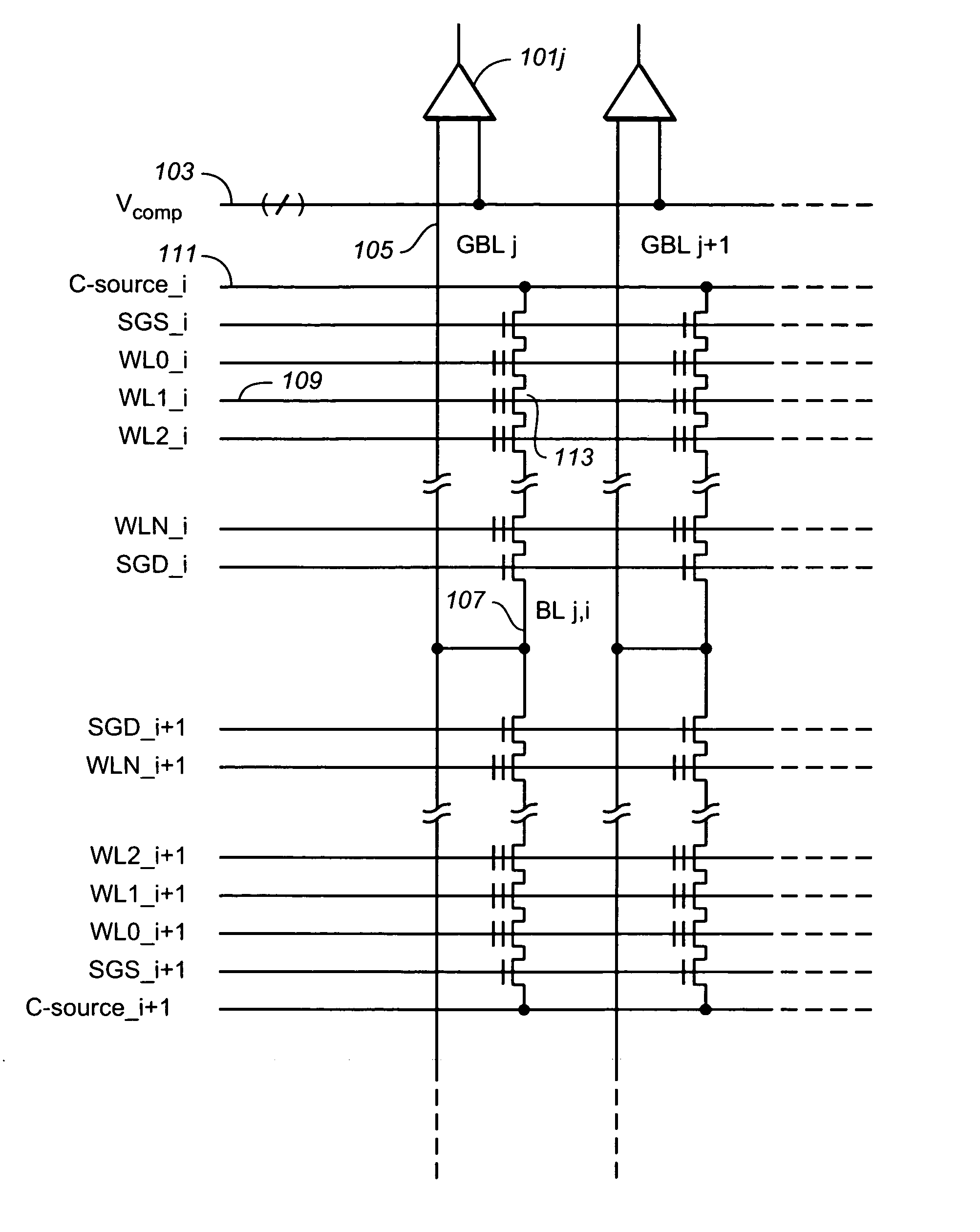
[0010] Briefly and generally, the present invention presents a scheme for sensing memory cells that is particularly useful for improving performance in multi-level non-volatile memory systems. This is achieved by setting an initial state in selected memory cells by discharging their channels to ground, placing a voltage level on the traditional source (such as the common electrode that connects the same end of the NAND strings in one block together) and the control gate, and allowing the cell bit line to charge up for some time as a result of conduction of current through the cell during the signal integration period. The bit line of the memory cell will then charge up until the bit line voltage becomes sufficiently high enough to shut off any further cell conduction. The rise of the bit line voltage will occur at a rate and to a level dependent upon the data state of the cell, and the cell will then shut off when the bit line, which now plays the role of the source for the NAND string, voltage reaches a high enough level such that the body effect affected memory cell threshold is reached at which point the current essentially shuts off. More specifically, an exemplary embodiment uses this technique for sensing in both the verify phase of write operations and for read operations. A plurality of cells along the same word line are sensed concurrently by placing. a constant, data independent voltage on the word line and constant, data independent common voltage level on the source side of these cells. The source side is now playing the role of the drain in the sense that its voltage is higher than the bit line side. The bit lines of cells, having previously been discharged, will then cause a voltage on their respective bit lines indicative of their individual data content.
[0011] In a sub-aspect of the present invention, the present invention allows for a single pass of verify operation to verify the state of all cells being programmed, regardless of the cells target state. As the level to which the corresponding bit line will rise depends, due to the body effect, upon the state of the cell. This level can then be compared against the reference value corresponding to the respective target values. This improves performance over prior art techniques requiring multiple charge-discharge, and signal integration cycles following each program pulse, one cycle for each target state requiring a verify operation.
[0012] In another sub-aspect of the present invention, read performance is improved as all data levels can be determined based upon the single discharge-charge cycle. As the level on a given cells bit line approaches an asymptotic value determined by the data content, once these levels are reached the level on the bit line can be compared to a set of reference levels, the comparison phase performed either sequentially or concurrently.
[0013] In a further sub-aspect of the present invention, and in one set of embodiments, the peripheral circuitry supplies the reference voltages to the bit line comparators sequentially. The reference values can all be available concurrently to a multiplexing circuit that supplies the different value, or the line supplying the reference values to the comparator can itself receive the various reference values in a time multiplexed manner. Although this last technique requires the changing of the voltage level on the reference supply line, this can be effected more rapidly than recharging and discharging the bit lines for each data level.
[0014] Another aspect of the present invention is sensing the state of the multi-state memory cells by performing multiple sensing sub-operations, each with a different control gate voltage, but with multiple states being sensed in each operation by charging the previously discharged cells up through their source. By combining elements of the two diverse sensing techniques, the sensing operation is sped up, as multiple states are read in each sensing sub-operation, while the use of multiple word line voltages provides sufficient dynamic range to resolve all of the data states.

Problems solved by technology

Actual shifts in the charge stored in one cell can be disturbed when reading, programming and erasing other cells that have some degree of electrical coupling with that cell, such as those in the same column or row, and those sharing a line or node.
The problem occurs most pronouncedly between two sets of adjacent cells that have been programmed at different times. One set of cells is programmed to add a level of charge to their floating gates that corresponds to one set of data.

Method used


Image

  • Alternate sensing techniques for non-volatile memories
  • Alternate sensing techniques for non-volatile memories
  • Alternate sensing techniques for non-volatile memories

Examples


Embodiment Construction

Example Non-Volatile Memory System

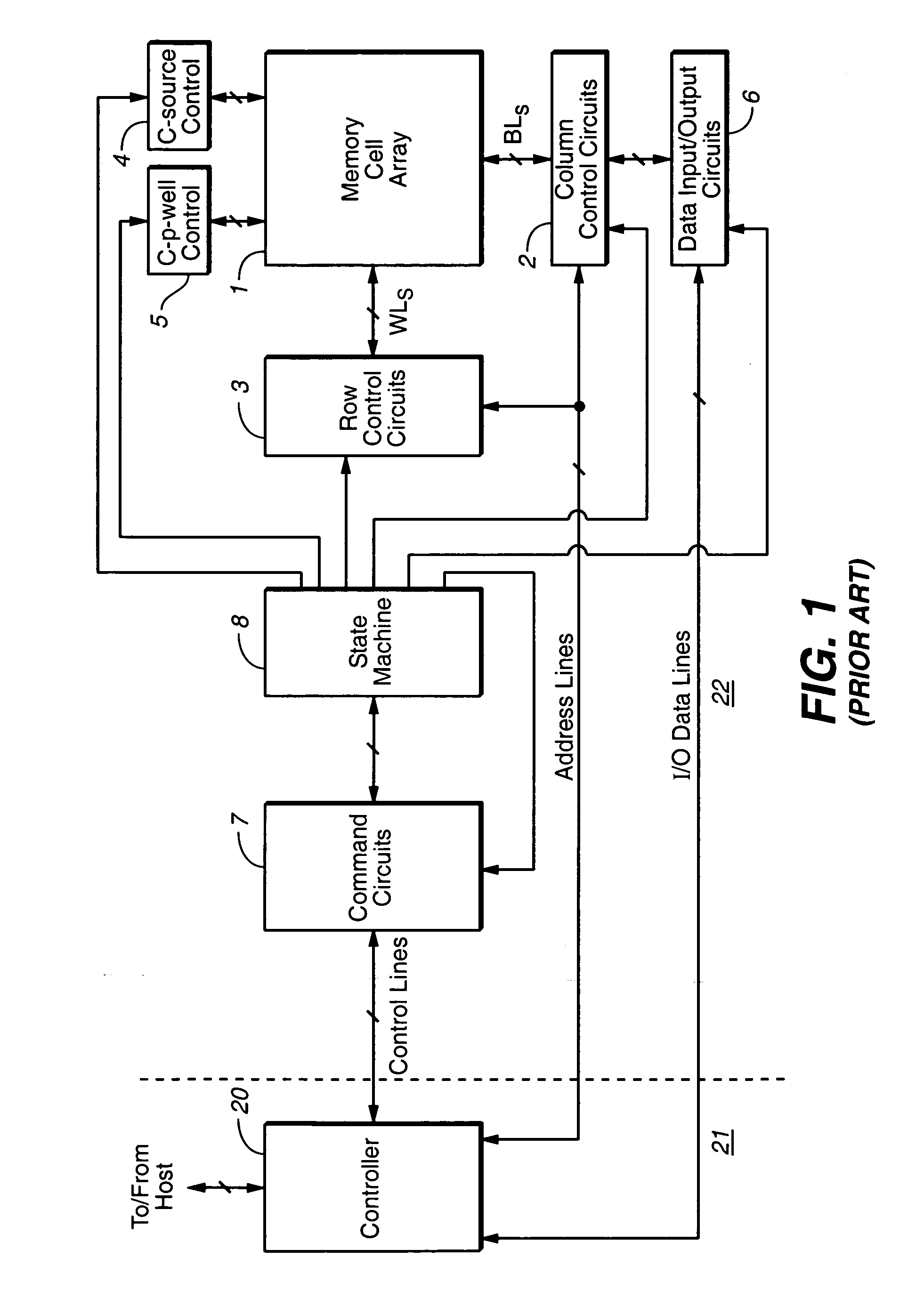
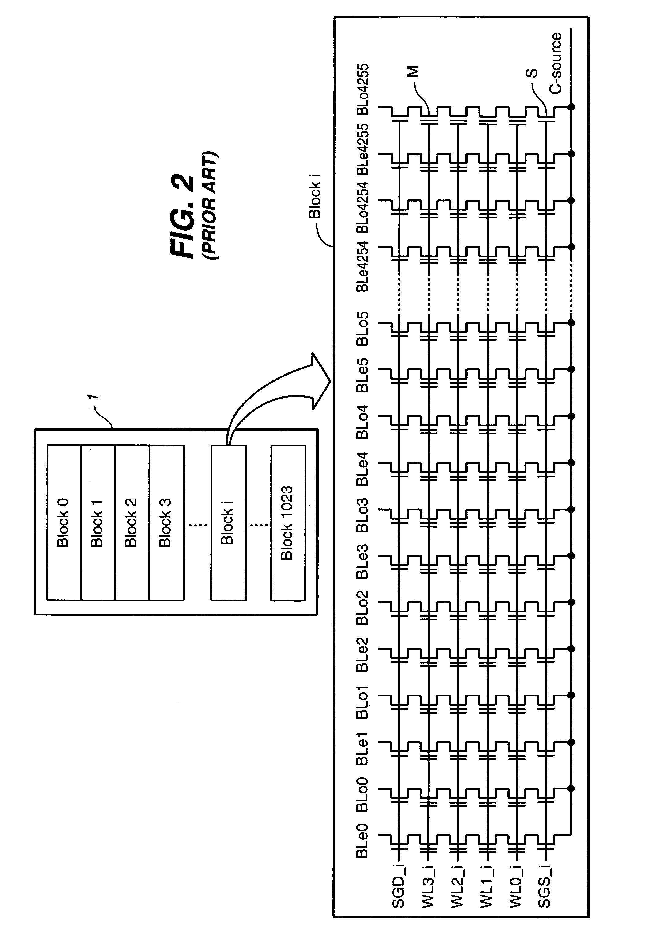
[0031] With reference to FIGS. 1-7, a specific non-volatile memory system is described in which the various aspects of the present invention are implemented, in order to provide definite examples. FIG. 1 is a block diagram of a flash memory system. Memory cell array 1 including a plurality of memory cells M arranged in a matrix is controlled by a column control circuit 2, a row control circuit 3, a c-source control circuit 4 and a c-p-well control circuit 5. The column control circuit 2 is connected to bit lines (BL) of the memory cell array 1 for reading data stored in the memory cells (M), for determining a state of the memory cells (M) during a program operation, and for controlling potential levels of the bit lines (BL) to promote the programming or to inhibit the programming. The row control circuit 3 is connected to word lines (WL) to select one of the word lines (WL), to apply read voltages, to apply program voltages combined with the bit l...


PUM


Abstract

The present invention presents a scheme for sensing memory cells. Selected memory cells are discharged through their channels to ground and then have a voltage level placed on the traditional source and another voltage level placed on the control gate, and allowing the cell bit line to charge up. The bit line of the memory cell will then charge up until the bit line voltage becomes sufficiently high to shut off any further cell conduction. The rise of the bit line voltage will occur at a rate and to a level dependent upon the data state of the cell, and the cell will then shut off when the bit line reaches a high enough level such that the body effect affected memory cell threshold is reached, at which point the current essentially shuts off. A particular embodiment performs multiple such sensing sub-operations, each with a different control gate voltage, but with multiple states being sensed in each operation by charging the previously discharged cells up through their source.

Description

CROSS-REFERENCE TO RELATED APPLICATION [0001] The present application is related to U.S. application Ser. No. ______ of Nima Mokhlesi et al., entitled “Memories With Alternate Sensing Techniques,” which is filed concurrently with the present application and is hereby incorporated herein, in its entirety, by this reference. FIELD OF THE INVENTION [0002] This invention relates generally to non-volatile memories and their operation, and, more specifically, to techniques for reading such memories. BACKGROUND OF THE INVENTION [0003] The principles of the present invention have application to various types of non-volatile memories, those currently existing and those contemplated to use new technology being developed. Implementations of the present invention, however, are described with respect to a flash electrically erasable and programmable read-only memory (EEPROM), wherein the storage elements are floating gates, as exemplary. [0004] It is common in current commercial products for eac...

Claims


Application Information

Patent Timeline
IPC IPC(8): G11C16/04G11C16/06G11C11/34
CPCG11C16/28
Inventor MOKHLESI, NIMALUTZE, JEFFREY W.
Owner WODEN TECH INC
Learn More