
Level shift delay equalization circuit and methodology

a delay equalization and level technology, applied in the field of level shifters, can solve the problems of causing a first delay and causing a greater delay

Active Publication Date: 2007-06-28
ANALOG DEVICES INT UNLTD
View PDF5 Cites 9 Cited by
  • Summary
  • Abstract
  • Description
  • Claims
  • Application Information

AI Technical Summary

Benefits of technology

The patent describes a circuit that can equalize delays in a level shift circuit. The circuit generates three signals that are related to the input signal in different ways. When the input signal changes from high to low, the circuit selects the signal that is inversely related to the input signal to control the output. This helps to reduce delays in the output. The circuit also includes a logic circuit that prevents the output from being simultaneously connected to two voltage reference nodes. The result is a more efficient and faster circuit that can equalize delays and reduce them to the shortest possible time.

Problems solved by technology

The first variable signal line incurs a first delay in transitioning from a high state level to a low state level and incurs a greater delay in transitioning from a low state level to a high state level.

Method used


Image

  • Level shift delay equalization circuit and methodology
  • Level shift delay equalization circuit and methodology
  • Level shift delay equalization circuit and methodology

Examples


Embodiment Construction

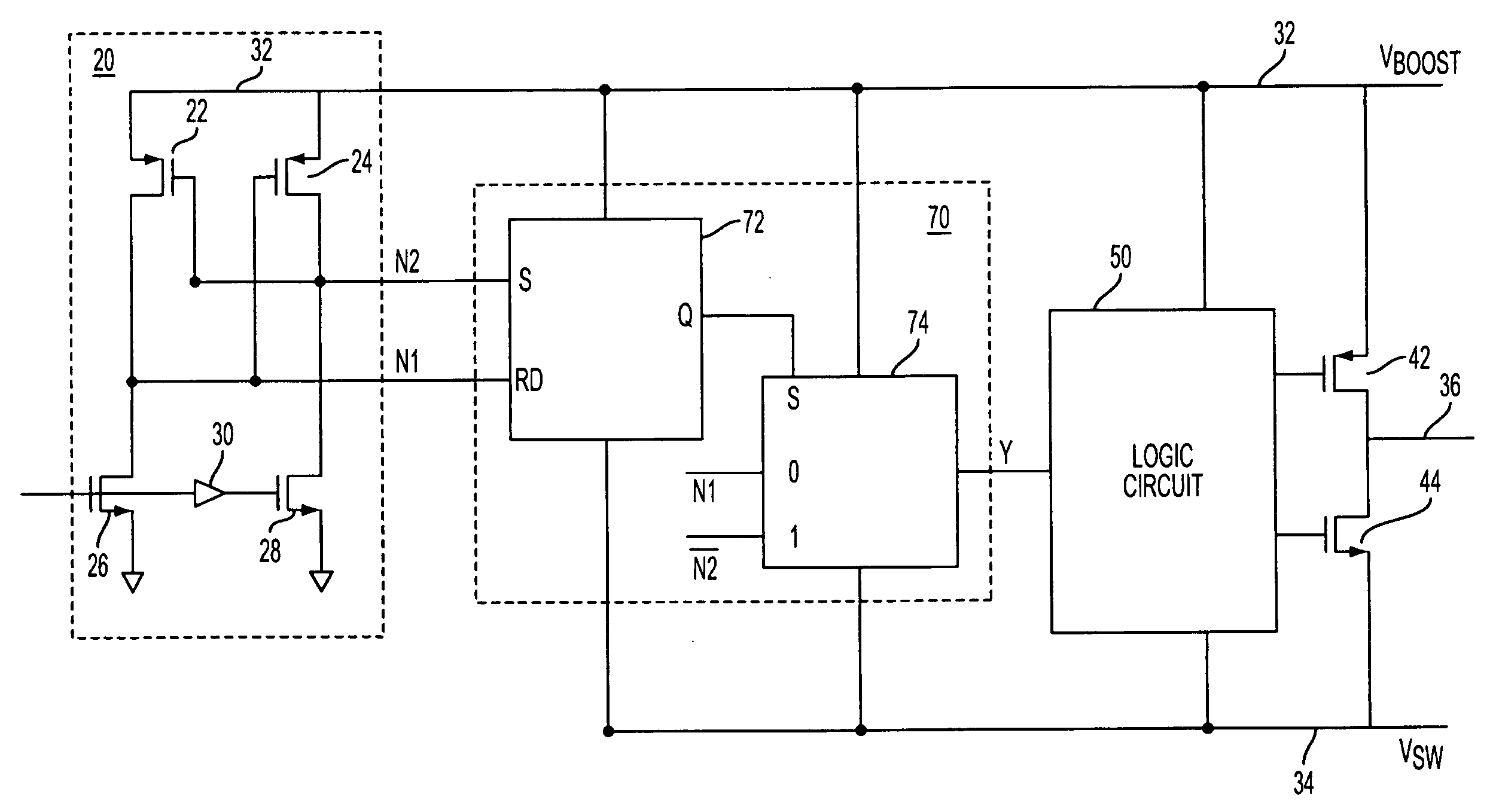
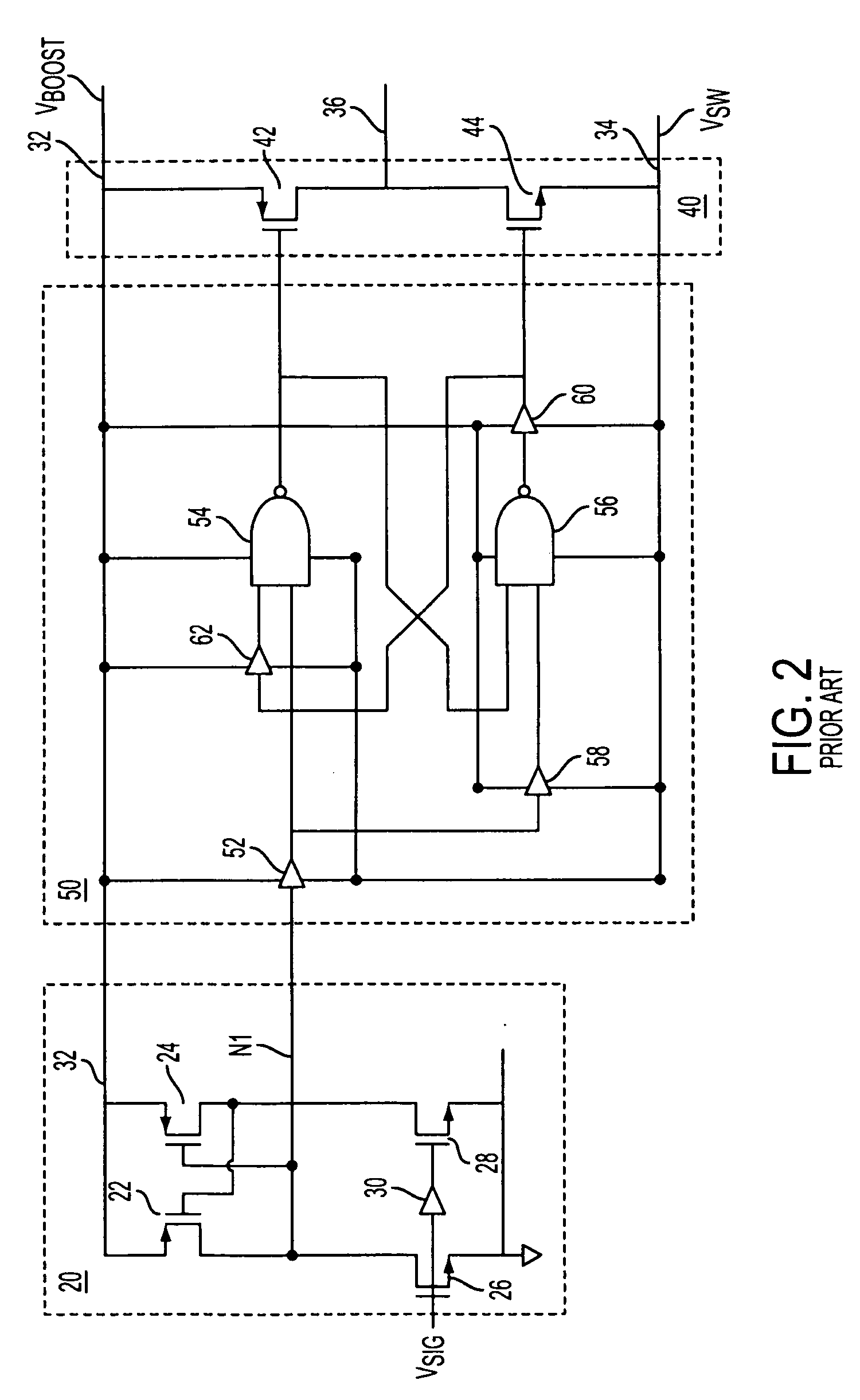
[0022] A delay equalization circuit 70 is shown in FIG. 4, interposed between input stage 20 and logic circuit 50 of the level shifting circuit. Input stage 20 and logic circuit 50 may comprise the same circuit element configurations as shown in prior art FIG. 2. Circuit 70 uses the fast High-to-Low transitions on N1 to control the Low-to-High transition of V36 and the High-to-Low transitions on N2 to control the High-to-Low transition of V36.

[0023] Circuit 70 comprises reset dominant latch 72 and data selection circuit 74. Line N1 is coupled to the reset input of latch 72. A line N2 is coupled to the set input of the latch. Line N2 is also coupled to the drain of FET 24. FET 24 is conductive when the input signal is at a high state and is nonconductive when the input signal is at a low state. The Q output of latch 72 is coupled to a select input, S, of data selection circuit 74. A line having the same signal state as N1 is coupled to a 0 input of the data selection circuit. A line...


PUM


Abstract

Transition delays in a level shift circuit are equalized by generating a first signal related to the state of the input signal, a second signal inversely related to the state of the input signal, and a third signal that is reciprocal to the second signal. Upon transition of the input signal from a high state to a low state, the third signal is selected for controlling the output until the first signal attains a high state. The first signal is selected for controlling the output when it has reached a high state after the input signal transition. The first signal remains selected upon transition of the input signal from a high state to a low state. Thus, output delays are equalized and reduced to the shortest delay.

Description

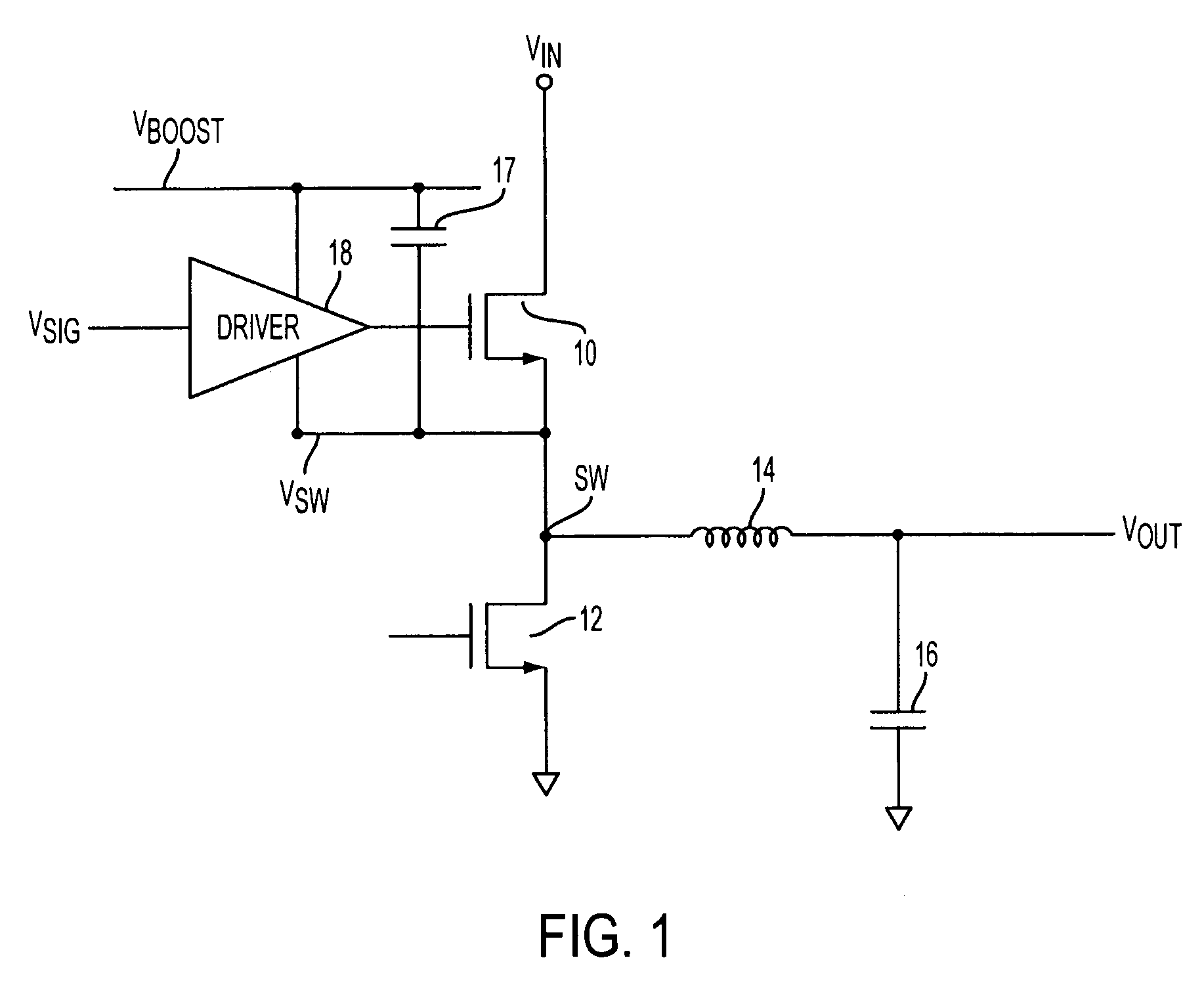
TECHNICAL FIELD [0001] The present disclosure relates to level shifters, more particularly to the control of output delays incurred upon transitioning between level states. BACKGROUND [0002] Level shifters are utilized in a variety of applications in which it is desired to couple a circuit node to either of two voltage levels in dependence upon the state of an input control signal. FIG. 1 is a simplified illustration of a driver applied to a high side FET of a buck converter. The converter comprises FETs 10 and 12, inductor 14 and capacitor 16. The junction of FETs 10 and 12 and inductor 14 is indicated as SW. Various other converter and controller elements are not shown as they are not necessary for explanation of the broad operation. Output VOUT of the converter is maintained at a lower voltage level than the input voltage VIN. FETs 10 and 12 are alternatively activated in succession. As VIN is greater than VOUT, activation of FET 10 permits charging of output capacitor 16 through...

Claims


Application Information

Patent Timeline
Patent Type & Authority Applications(United States)
IPC IPC(8): H03K19/094
CPCH03K19/0013H03K19/00323
Inventor PRICE, BURT LEE
Owner ANALOG DEVICES INT UNLTD
Learn More