
MIM capacitor and method of fabricating same

a technology of capacitors and capacitors, applied in the direction of semiconductor devices, semiconductor/solid-state device details, electrical apparatus, etc., can solve the problems of adding considerable cost and time to the manufacture of integrated circuits incorporating mims

Active Publication Date: 2007-05-24
GLOBALFOUNDRIES U S INC
View PDF11 Cites 11 Cited by
  • Summary
  • Abstract
  • Description
  • Claims
  • Application Information

AI Technical Summary

Benefits of technology

This approach simplifies and reduces the cost of integrating MIMs into integrated circuits by allowing their fabrication in wiring levels alongside existing structures, thereby streamlining the manufacturing process.

Problems solved by technology

Current methods of integration of MIMs into integrated circuits require multiple extra photolithographic and etching steps beyond those required for all other components of the integrated circuits thus adding considerable cost and time to the manufacture of integrated circuits incorporating MIMs.

Method used


Image

  • MIM capacitor and method of fabricating same
  • MIM capacitor and method of fabricating same
  • MIM capacitor and method of fabricating same

Examples


fourth embodiment

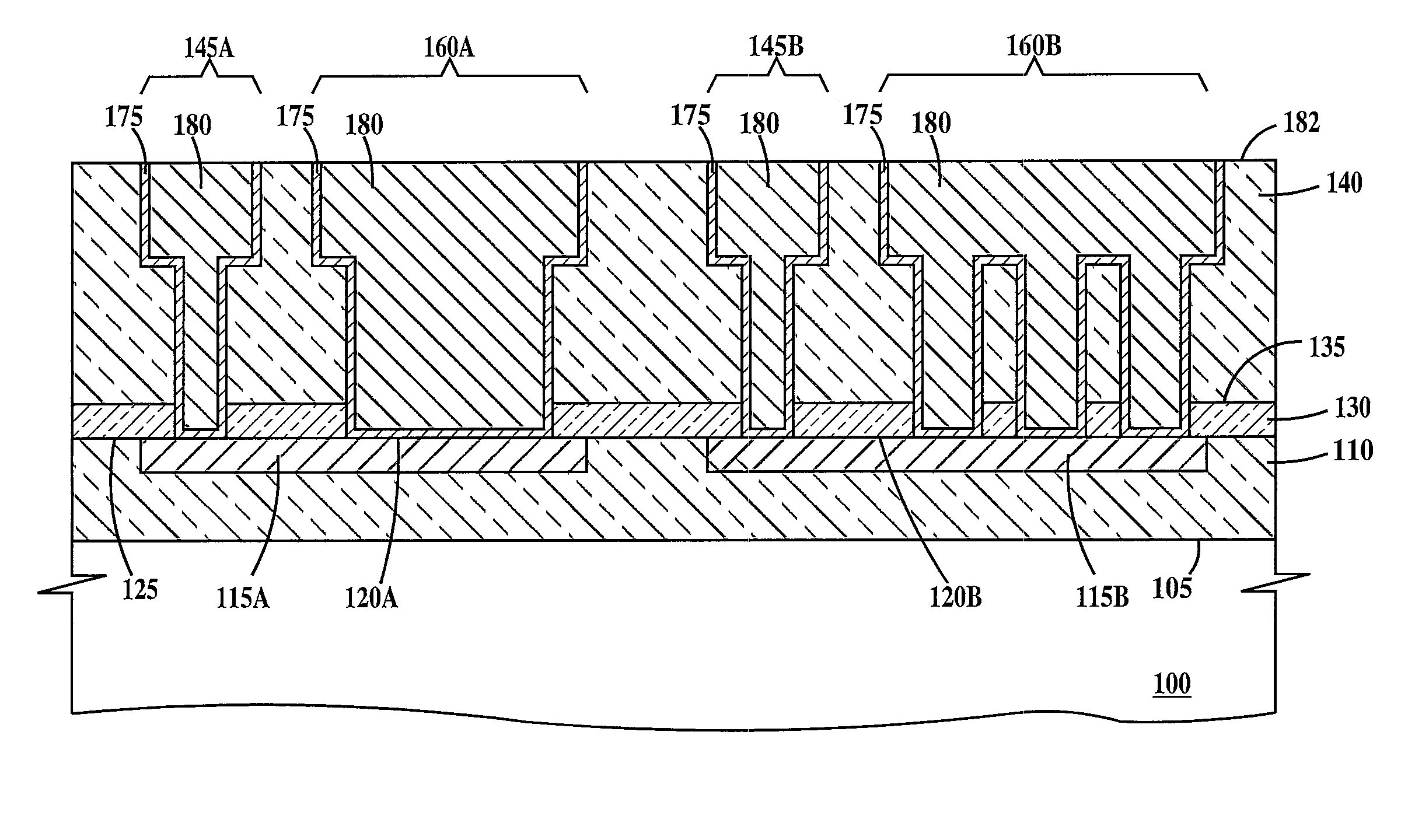
[0031]FIG. 2E is a cross-sectional drawings illustrating steps for manufacture of MIM capacitor devices according to a third and the present invention. In FIG. 2E, a first device 200C comprises a MIM capacitor 205C, a contact 210C and conductor 115A. A first plate of MIM capacitor 205C comprises core conductor 195. A second device 200D comprises a MIM capacitor 205D, a contact 210D and conductor 115B. A second plate of MIM capacitor 205D comprises conductive liner 175.

[0032] In FIG. 2E, an optional recess process is performed to recess core conductors 180 and 195 below surface 183. This reduces the possibility of shorts between conductive liner 175 and core conductor 195. In one example, the recess process is a wet etch using an etchant comprising HNO3, HCl, H2SO4, HF or combinations thereof. In a second example, the CMP process used to generate the structures of FIG. 2D are adjusted to cause dishing in at least core conductor 195 of MIM capacitors 205C and 205D. Dishing is phenomen...

eighth embodiment

[0039]FIG. 3E is a cross-sectional drawings illustrating steps for manufacture of MIM capacitor devices according to a seventh and the present invention. In FIG. 3E, a first device 220C comprises a MIM capacitor, a contact 230C and conductor 115A. A first plate of MIM capacitor 225C comprises core conductor 195. The insulator of MIM capacitor 225C comprises dielectric layer 190. A first portion of a second plate of MIM capacitor 225C comprises conductive liner 175. Remaining conductor 180 comprises a second portion of second plate of MIM capacitor 225C.

[0040] A second device 220D comprises a MIM capacitor 225B, a contact 230D and conductor 115B. A first plate of MIM capacitor 225D comprises core conductor 195. The insulator of MIM capacitor 225D comprises dielectric layer 190. A first portion of a second plate of MIM capacitor 225D comprises conductive liner 175. Remaining conductor 180 comprises a second portion of second plate of MIM capacitor 225D. Electrical connection between t...


PUM


Abstract

A damascene MIM capacitor and a method of fabricating the MIM capacitor. The MIN capacitor includes a dielectric layer having top and bottom surfaces; a trench in the dielectric layer, the trench extending from the top surface to the bottom surface of the dielectric layer; a first plate of a MIM capacitor comprising a conformal conductive liner formed on all sidewalls and extending along a bottom of the trench, the bottom of the trench coplanar with the bottom surface of the dielectric layer; an insulating layer formed over a top surface of the conformal conductive liner; and a second plate of the MIM capacitor comprising a core conductor in direct physical contact with the insulating layer, the core conductor filling spaces in the trench not filled by the conformal conductive liner and the insulating layer. The method includes forming portions of the MIM capacitor simultaneously with damascene interconnection wires.

Description

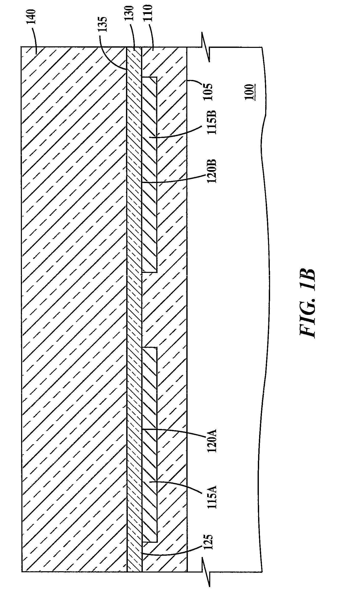
RELATED APPLICATIONS [0001] This application is a division of copending U.S. application Ser. No. 11 / 106,887 filed on Apr. 15, 2005.FIELD OF THE INVENTION [0002] The present invention relates to the field of integrated circuits and integrated circuit fabrication; more specifically, it relates to metal-insulator-metal capacitor and a method of fabricating the metal-insulator-metal capacitor. BACKGROUND OF THE INVENTION [0003] Metal-insulator-metal capacitors (MIM or MIM cap) are integrated into various integrated circuits for applications such as analog-logic, analog-to-digital, mixed signal and radio frequency circuits. Current methods of integration of MIMs into integrated circuits require multiple extra photolithographic and etching steps beyond those required for all other components of the integrated circuits thus adding considerable cost and time to the manufacture of integrated circuits incorporating MIMs. [0004] Thus, there is a need for a simple and inexpensive integration s...

Claims


Application Information

Patent Timeline
Patent Type & Authority Applications(United States)
IPC IPC(8): H01L21/8242H01L29/94H01L27/108H10B12/00
CPCH01L23/5223H01L23/5329H01L23/53295H01L2924/0002H01L2924/00
Inventor YANG, CHIH-CHAOCLEVENGER, LAWRENCE A.DALTON, TIMOTHY J.HSU, LOUIS C.
Owner GLOBALFOUNDRIES U S INC
Learn More