
Light emitting device

a technology of light-emitting devices and substrates, which is applied in the field of light-emitting devices, can solve the problems of difficult cracking of films on plastic substrates, and achieve the effect of preventing deterioration of substrates and flexible substrate structures

Inactive Publication Date: 2007-05-24
SEMICON ENERGY LAB CO LTD
View PDF76 Cites 36 Cited by
  • Summary
  • Abstract
  • Description
  • Claims
  • Application Information

AI Technical Summary

Benefits of technology

The present invention provides a light emitting device using a plastic material as a substrate, which is capable of preventing the substrate from deterioration with the transmission of oxygen or moisture content. A lamination layer is formed on the principle surface of a substrate made of a plastic material to prevent the substrate from deterioration with the transmission of oxygen or moisture content. The lamination layer is made of one unit or two or more units, each unit being a laminated structure of a metal layer and an organic compound layer. The inorganic compound layer is formed so as to cover the end face of the lamination layer. The light emitting device comprises light emitting elements formed between the lamination layer and an inorganic compound layer that transmits visual light. A thin film transistor connected to the light emitting element can be formed in matrix form to provide a pixel portion. The inorganic compound layer can be formed so as to cover the end face of the lamination layer. The lamination layer can be made of aluminum or aluminum alloy, and the organic compound layer can be made of a heat-curable or photo-curable resin material. The light emitting device can be used in various applications such as displays and lighting devices.

Problems solved by technology

In this case, there is a need of forming the film of 5 nm or less in thickness and making the film difficult to be cracked when the plastic substrate is bent.

Method used


Image

  • Light emitting device
  • Light emitting device
  • Light emitting device

Examples


embodiment 1

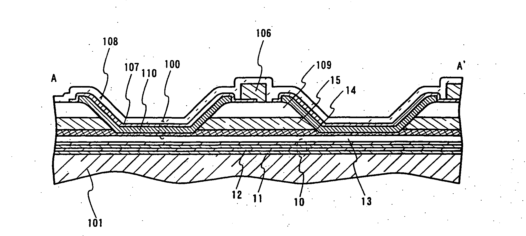
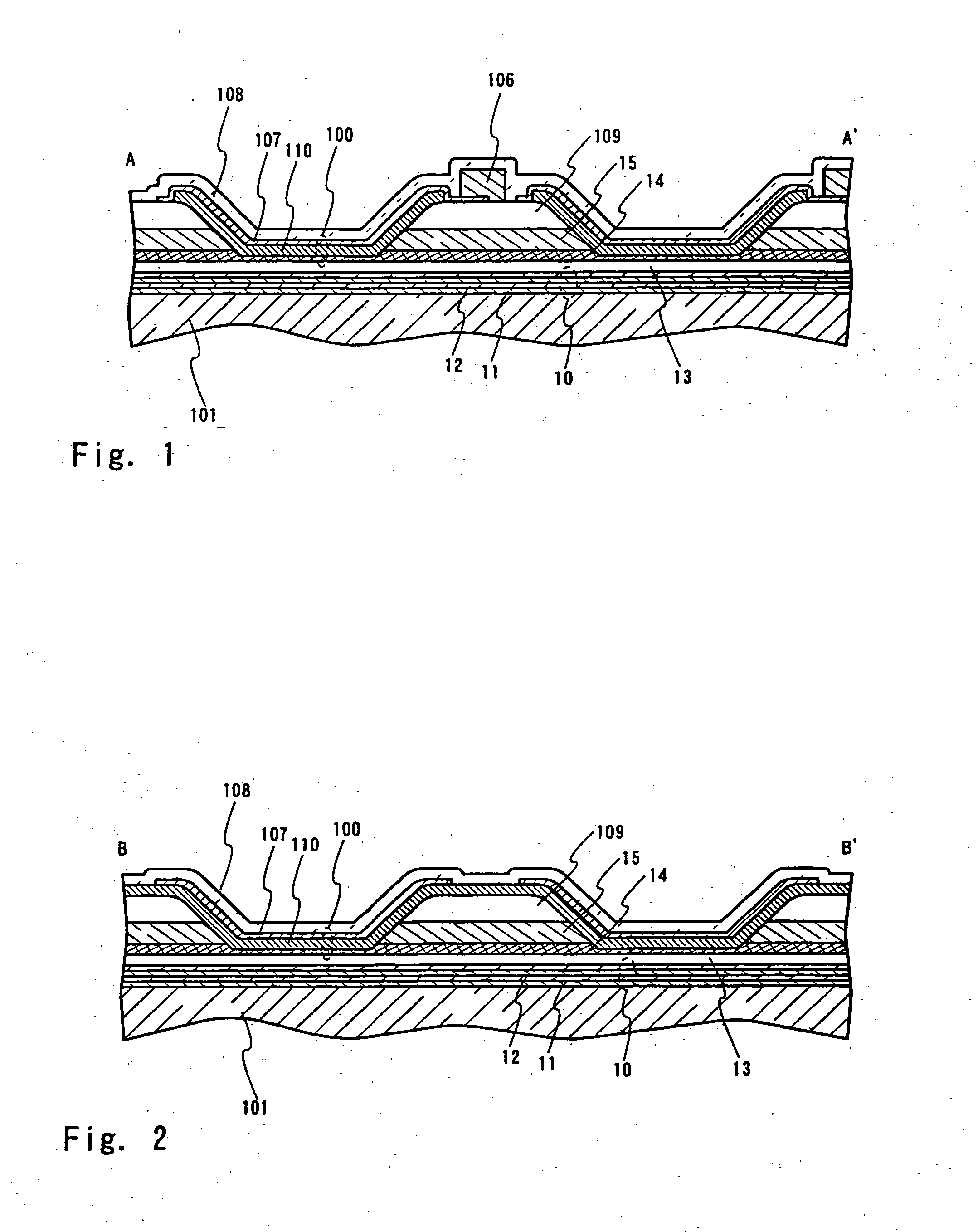
[0051] In this embodiment, a light emitting device is of a simple matrix type, in which light emitting elements are arranged in a matrix form to constitute a display screen. In this embodiment, we will describe an embodiment of sealing structure for protecting the light emitting elements from external contaminations such as oxygen and water vapor.

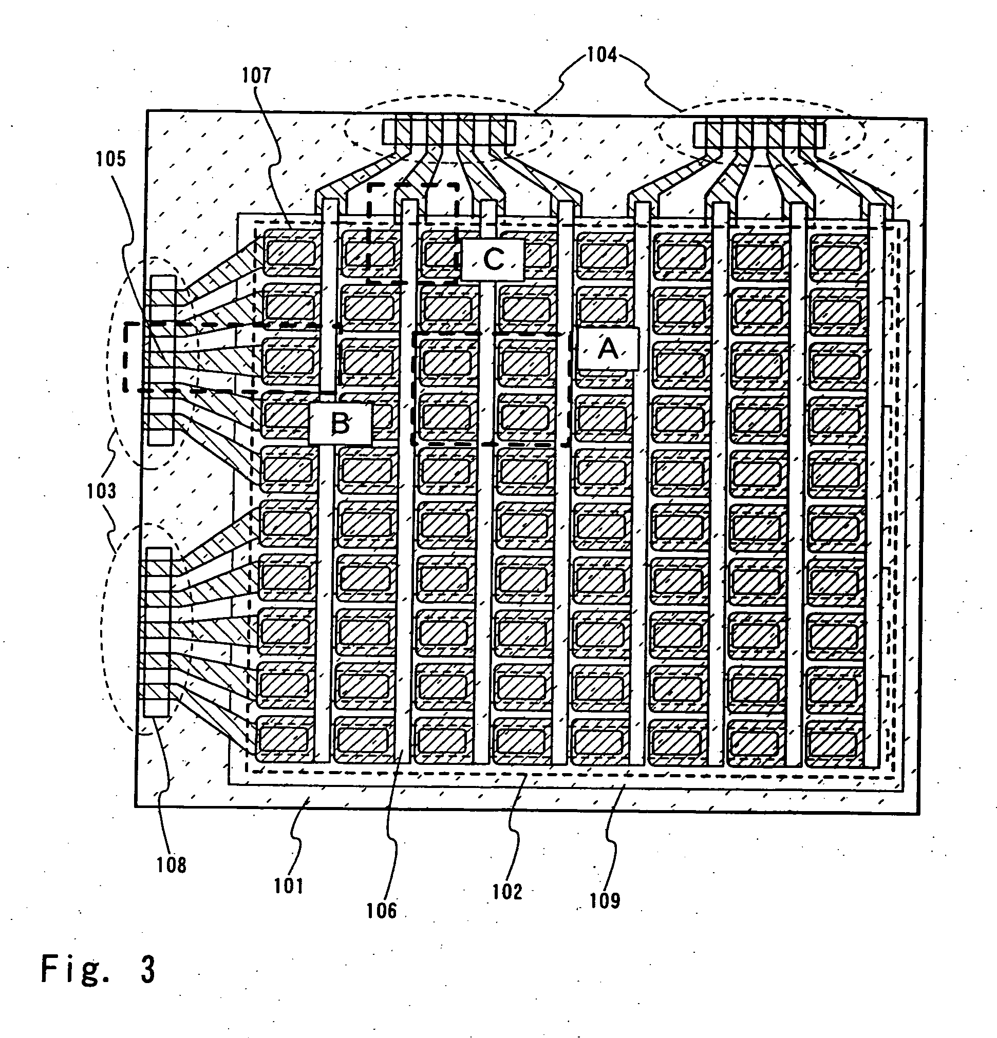
[0052]FIG. 3 is a top view for illustrating the configuration of the sealing structure. As shown in the figure, a pixel portion 102 is formed, where light emitting elements are arranged in a matrix form on a substrate 101. The pixel portion 102 includes a first wiring 105 in a stripe form extending in the X direction and a second wiring 106 in a stripe form extending in the Y direction. A first electrode 107 of the light emitting element is electrically connected to the second wiring 106. The stripe-formed first wiring 105 in the X direction and the stripe-formed second wiring 106 in the Y direction form their respective signal input termi...

embodiment 2

[0080] In this embodiment, a light-emitting device is in the type of an active matrix in which a light emitting element and a TFT for controlling the light emitting element are arranged on each pixel to drive. In this embodiment, we will describe an embodiment of sealing structure for preventing the light emitting elements and TFTs from external contaminations such as oxygen and water vapor.

[0081]FIG. 13 is a top view for illustrating a pixel structure of the light emitting device, showing an exemplified configuration thereof in which a TFT and a light emitting element are mounted. FIG. 14 is a vertical cross sectional view along the line E-E′ in FIG. 13. Therefore, the present embodiment will be described with reference to these figures. Furthermore, in FIG. 13, the upper layers on a second electrode (i.e., a partition wall layer, an EL layer, a first electrode, and an inorganic compound layer) are omitted for a simplification of the drawing.

[0082] As shown in the figure, a lamin...

embodiment 3

[0095] Various kinds of electronic apparatus can be implemented with the light emitting device of the present invention described above. Typical electronic apparatus includes personal digital assistants (i.e., electronic notes, mobile computers, cellular phones, and electronic books and magazines), video cameras, digital cameras, cellular phones, and so on. Some of these examples are shown in FIG. 20.

[0096] In FIG. 20A, there is shown an example of a video camera implemented by the application of the present invention. The video camera comprises a main body 3011, a display part 3012, a voice input part 3013, an operation switch 3014, a battery unit 3015, and a viewing part 3016. Accordingly, the present invention allows the implementation of such a light-weighted video camera.

[0097] In FIG. 20B, there is shown an example of a personal digital assistant (PDA) implemented by the application of the present invention. The PDA comprises a main body 3031, a stylus pen 3032, a display pa...


PUM


Abstract

A light emitting device having a plastic substrate is capable of preventing the substrate from deterioration with the transmission of oxygen or moisture content can be obtained. The light emitting device has light emitting elements formed between a lamination layer and an inorganic compound layer that transmits visual light, where the lamination layer is constructed of one unit or two or more units, and each unit is a laminated structure of a metal layer and an organic compound layer. Alternatively, the light emitting device has light emitting elements formed between a lamination layer and an inorganic compound layer that transmits visual light, where the lamination layer is constructed of one unit or two or more units, and each unit is a laminated structure of a metal layer and an organic compound layer, wherein the inorganic compound layer is formed so as to cover the end face of the lamination layer. In the present invention, the lamination layer is formed on the primary surface of the plastic substrate, so that a flexible substrate structure can be obtained while preventing the substrate from deterioration with the transmission of oxygen or moisture content.

Description

BACKGROUND OF THE INVENTION [0001] 1. Field of the Invention [0002] The present invention relates to a light emitting device using an organic compound material as a luminescent material, and in particular, to the configuration of a light emitting device in which a plastic material is used as a substrate. [0003] 2. Description of the Related Art [0004] Heretofore, a light emitting device utilizing a luminescence phenomenon with electroluminescence (hereinafter, referred to as EL) has been investigated so as to be applied as a means for forming image that represents information such as characters and images. Among inorganic compound materials, zinc sulfide has been known as a typical luminescent material (EL material) that generates EL. On the other hand, among organic compound materials, an aluminum tris(8-hydroxyquinoline) (Alq3) complex has been known as a typical EL material. [0005] The light emitting element using such an EL material has a comparatively simple structure and conta...

Claims


Application Information

Patent Timeline
Patent Type & Authority Applications(United States)
IPC IPC(8): H01L33/00H01L31/12H01L27/32H10N10/856H01L51/52
CPCH01L27/3244H01L27/3274H01L27/3281H01L27/3288H01L51/5256H01L51/5262H01L51/5271H01L2251/5338H01L51/5253H01L51/52H10K59/12H10K59/125H10K59/17H10K59/179H10K2102/311H10K59/8731H10K59/878H10K10/466H10K50/80H10K50/844H10K50/856H10K50/8445H10K10/464H10K50/11H10K50/85H10K85/113B82Y10/00
Inventor YAMAZAKI, SHUNPEIARAI, YASUYUKI
Owner SEMICON ENERGY LAB CO LTD
Learn More