Electron emission device

Inactive Publication Date: 2007-05-03
SAMSUNG SDI CO LTD
View PDF8 Cites 8 Cited by
  • Summary
  • Abstract
  • Description
  • Claims
  • Application Information

AI Technical Summary

Benefits of technology

[0013] The present invention provides an electron emission device having enhanced electron emission uniformity and improved electron emission efficiency.

Problems solved by technology

However, when a width of each opening formed in the gate electrode and insulation is too small, it is difficult to form the electron emission region having a sufficient area and thus, the electron emission efficiency is reduced.

Method used


Image

  • Electron emission device
  • Electron emission device
  • Electron emission device

Examples


Embodiment Construction

[0025] The present invention is described more fully below with reference to the accompanying drawings, in which exemplary embodiments of the present invention are shown. The present invention can, however, be embodied in many different forms and should not be construed as being limited to the embodiments set forth herein; rather these embodiments are provided so that this disclosure will be thorough and complete, and will fully convey the concept of the present invention to those skilled in the art. Wherever possible, the same reference numbers are used throughout the drawings to refer to the same or like parts.

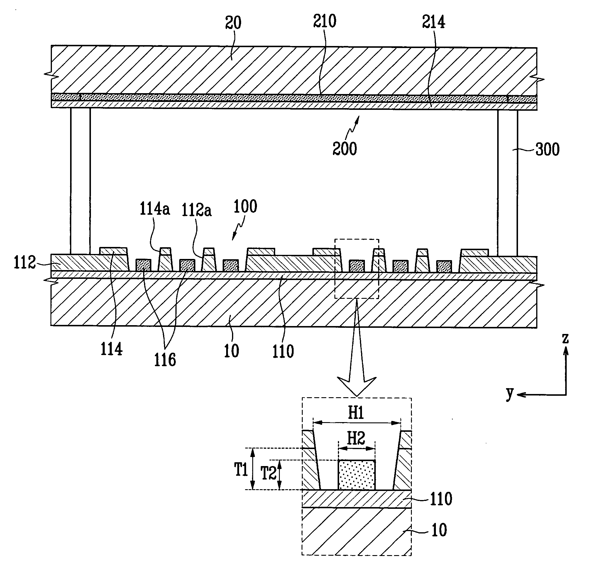
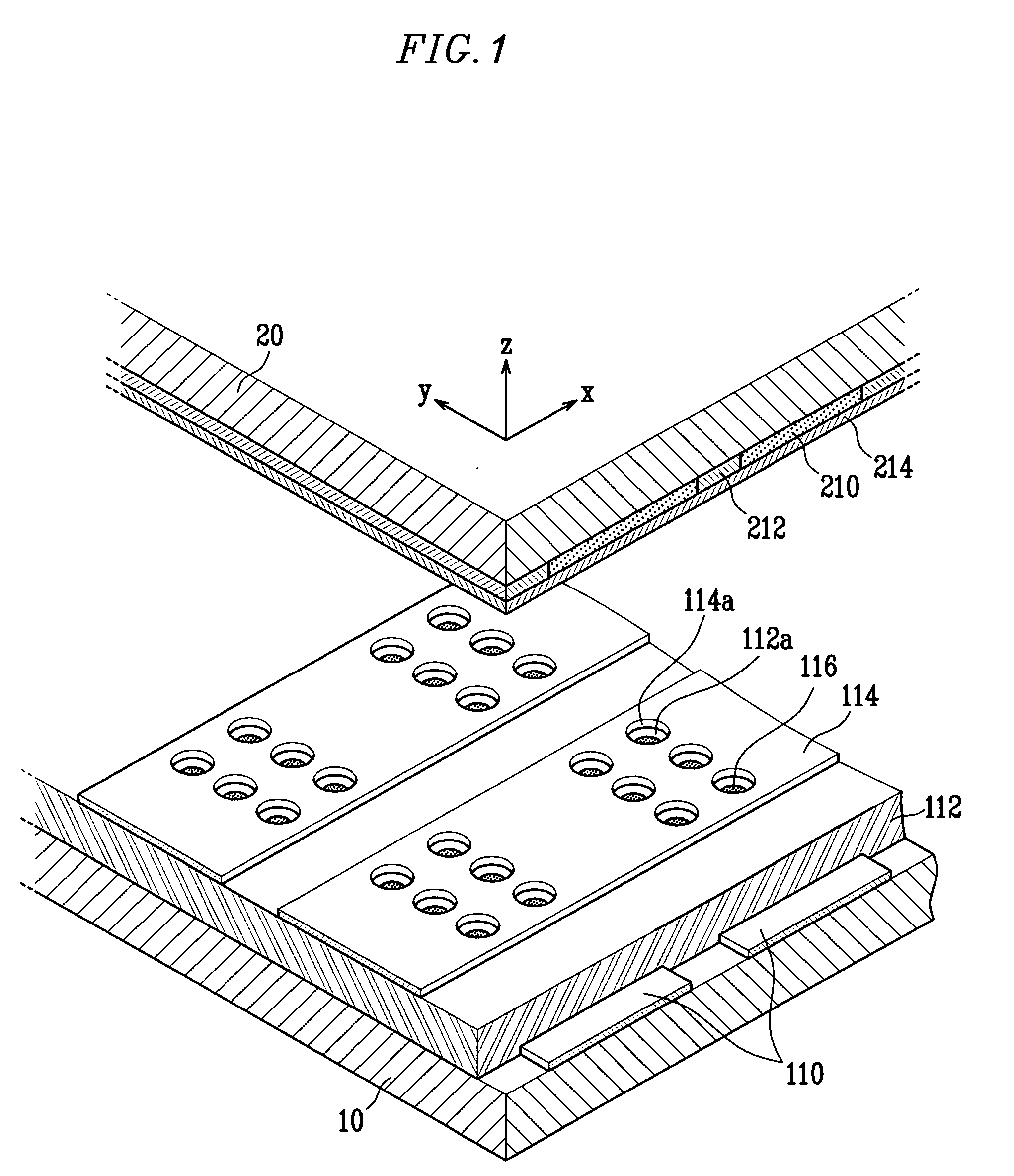
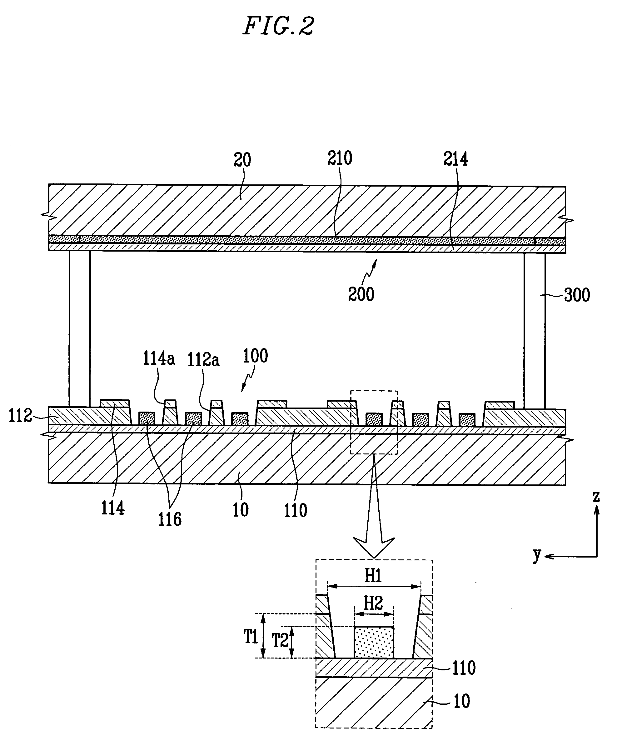
[0026]FIGS. 1, 2 and 3 are respectively partial exploded perspective, partial sectional, partial top views of an electron emission device according to an embodiment of the present invention.

[0027] Referring to FIGS. 1, 2 and 3, an electron emission device according to an embodiment of the present invention includes first and second substrates 10 and 20 facing each other an...


PUM


Abstract

An electron emission device is provided. The electron emission device includes first and second substrates facing each other, a cathode electrode arranged on the first substrate, at least one opening electron emission region arranged on the cathode electrode, an insulation layer arranged on the cathode electrode and provided with at least one opening corresponding to the at least one opening electron emission region, and a gate electrode arranged on the insulation layer and provided with at least one opening corresponding to the at least one electron emission region. A width H1 of the at least one opening of the insulation layer is equal to or greater than twice a thickness T1 of the insulation layer.

Description

CLAIM OF PRIORITY [0001] This application makes reference to, incorporates the same herein, and claims all benefits accruing under 35 U.S.C. §119 from an application for ELECTRON EMISSION DEVICE earlier filed in the Korean Intellectual Property Office on the 31 Oct. 2005 and there duly assigned Serial No. 10-2005-0103513. BACKGROUND OF THE INVENTION [0002] 1. Field of the Invention [0003] The present invention relates to an electron emission device having improved electron emission efficiency. [0004] 2. Description of the Related Art [0005] Generally, electron emission devices are classified into those using hot cathodes as an electron emission source, and those using cold cathodes as the electron emission source. [0006] There are several types of cold cathode electron emission elements, including Field Emitter Array (FEA) elements, Surface Conduction Emitter (SCE) elements, Metal-Insulator-Metal (MIM) elements, and Metal-Insulator-Semiconductor (MIS) elements. [0007] The FEA electr...

Claims


Application Information

Patent Timeline
IPC IPC(8): H01J63/04H01J1/62
CPCH01J1/304H01J3/021H01J29/481H01J31/127
Inventor LEE, SANG-JOLEE, CHUN-GYOOJEON, SANG-HOAHN, SANG-HYUCKHONG, SU-BONGSHIN, JONG-HOON
Owner SAMSUNG SDI CO LTD
Why Eureka
Try Eureka