Image pickup device mounting structure
- Summary
- Abstract
- Description
- Claims
- Application Information
AI Technical Summary
Benefits of technology
Problems solved by technology
Method used
Image

Examples
first embodiment
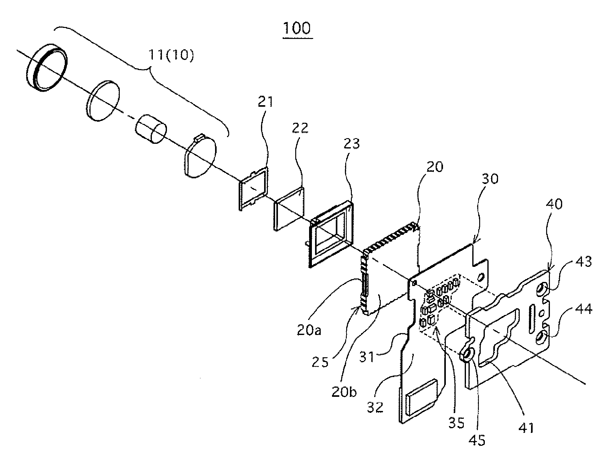
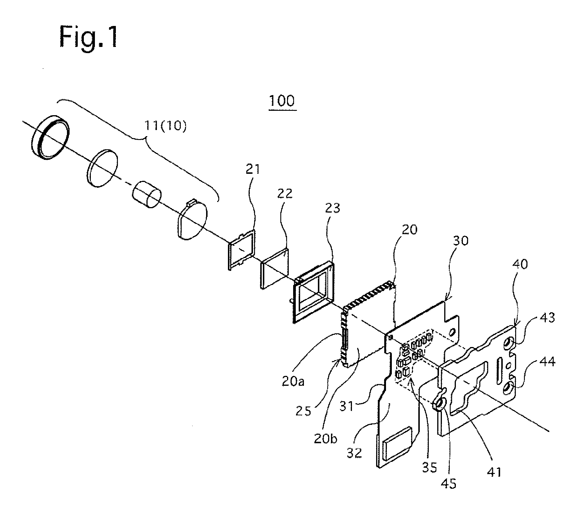
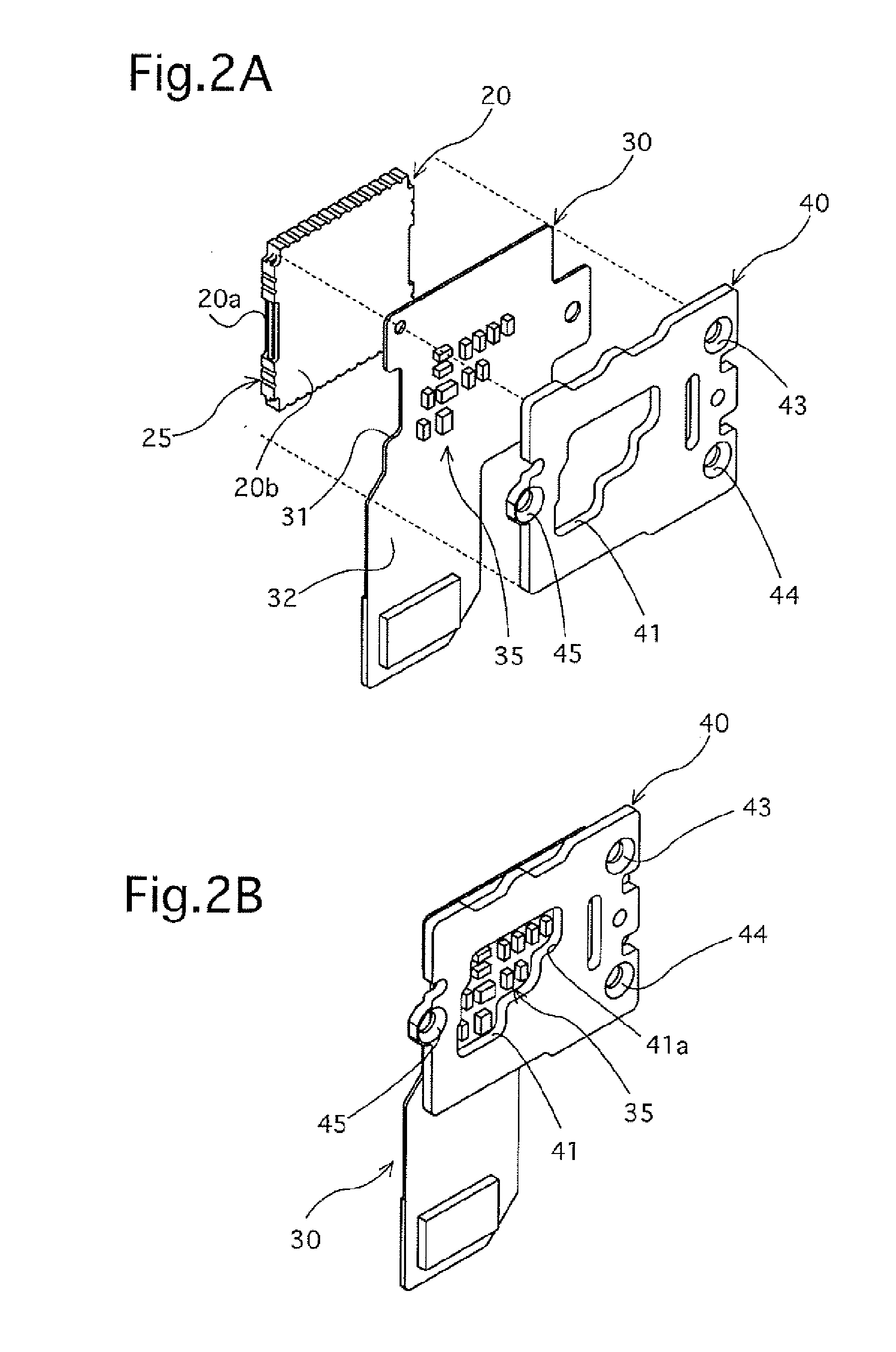
[0033]FIG. 1 shows main elements of a lens unit 100 which adopts a first embodiment of a mounting structure of an image pickup device to a flexible printed circuit board. The first embodiment of the mounting structure is provided with an image pickup device 20, a flexible PCB 30 and a reinforcing plate (mounting plate) 40. Light which emerges from a lens module 10 is incident on the image pickup device 20 to be focused thereon. The flexible PCB 30 is fixed to the image pickup device 20 and is electrically connected thereto. The lens module 10 is provided with a housing (not shown) and a plurality of lens elements 11 which are housed in the housing and supported thereby.
[0034] For instance, a surface-mount type of CCD (charge-coupled device) or CMOS (complementary metal oxide semiconductor), image sensor having a substantially rectangular shape in plan configuration, can be adopted as the image pickup device 20. The lens unit 100 is provided, in front of a front surface (imaging sur...
second embodiment
[0039] A second embodiment of the mounting structure will be discussed hereinafter. The second embodiment of the mounting structure shown in FIGS. 3A, 3B and 3C is different from the first embodiment of the mounting structure shown in FIGS. 1, 2A and 2B in that the second embodiment of the mounting structure is provided with an image pick up device 120, a flexible PCB 130 and a reinforcing plate 140 instead of the image pick up device 20, the flexible PCB 30 and the reinforcing plate 40 that are arranged from the lens module side, respectively. Apart from this difference, the second embodiment of the mounting structure has the same structure as the first embodiment of the mounting structure.
[0040] Similar to the flexible PCB 30, the flexible PCB 130 is provided with a flexible substrate and a plurality of conductor traces formed on one surface (front surface) 131 of the flexible PCB 130. A plurality of contacts 125 which project from the image pickup device 120 are soldered to a co...
PUM
 Abstract
Description
Claims
Application Information
 - R&D
- Intellectual Property
- Life Sciences
- Materials
- Tech Scout
- Unparalleled Data Quality
- Higher Quality Content
- 60% Fewer Hallucinations
Browse by: Latest US Patents, China's latest patents, Technical Efficacy Thesaurus, Application Domain, Technology Topic, Popular Technical Reports.
© 2025 PatSnap. All rights reserved.Legal|Privacy policy|Modern Slavery Act Transparency Statement|Sitemap|About US| Contact US: help@patsnap.com