Eureka AIR delivers breakthrough ideas for toughest innovation challenges, trusted by R&D personnel around the world.

Method of manufacturing image display device

Inactive Publication Date: 2007-04-19
KK TOSHIBA
View PDF0 Cites 2 Cited by
  • Summary
  • Abstract
  • Description
  • Claims
  • Application Information

AI Technical Summary

Benefits of technology

[0015] The method mentioned above uses expensive glass. For this reason, in the case of a large glass frame, cost of manufacture is high, high technical skill is required, and manufacturing efficiency is decreased.
[0016] Accordingly, the present invention has been made in the light of the above circumstances, and an object of the present invention is to provide a method of manufacturing an image display device which can be manufactured at low cost and easily.

Problems solved by technology

The method mentioned above uses expensive glass.
For this reason, in the case of a large glass frame, cost of manufacture is high, high technical skill is required, and manufacturing efficiency is decreased.

Method used


Image

  • Method of manufacturing image display device
  • Method of manufacturing image display device
  • Method of manufacturing image display device

Examples


Embodiment Construction

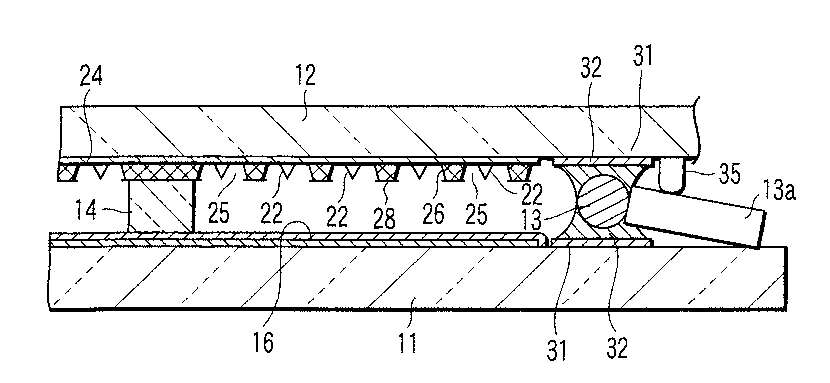
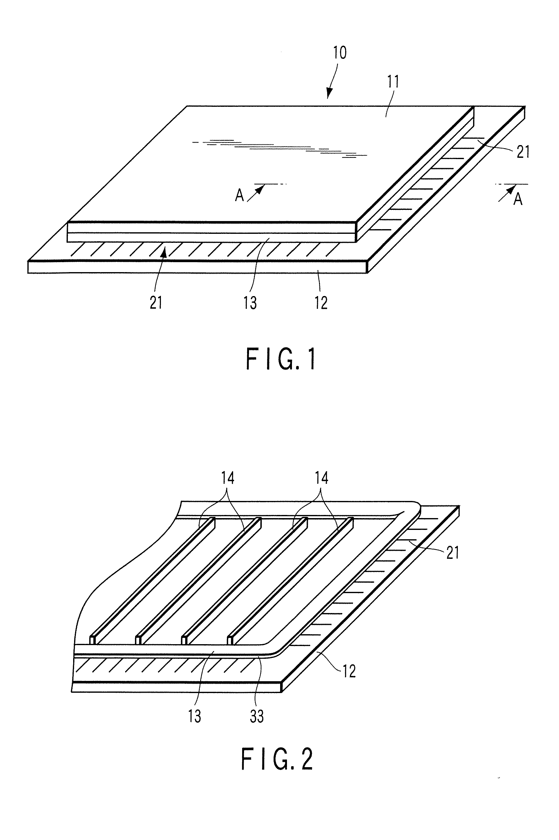
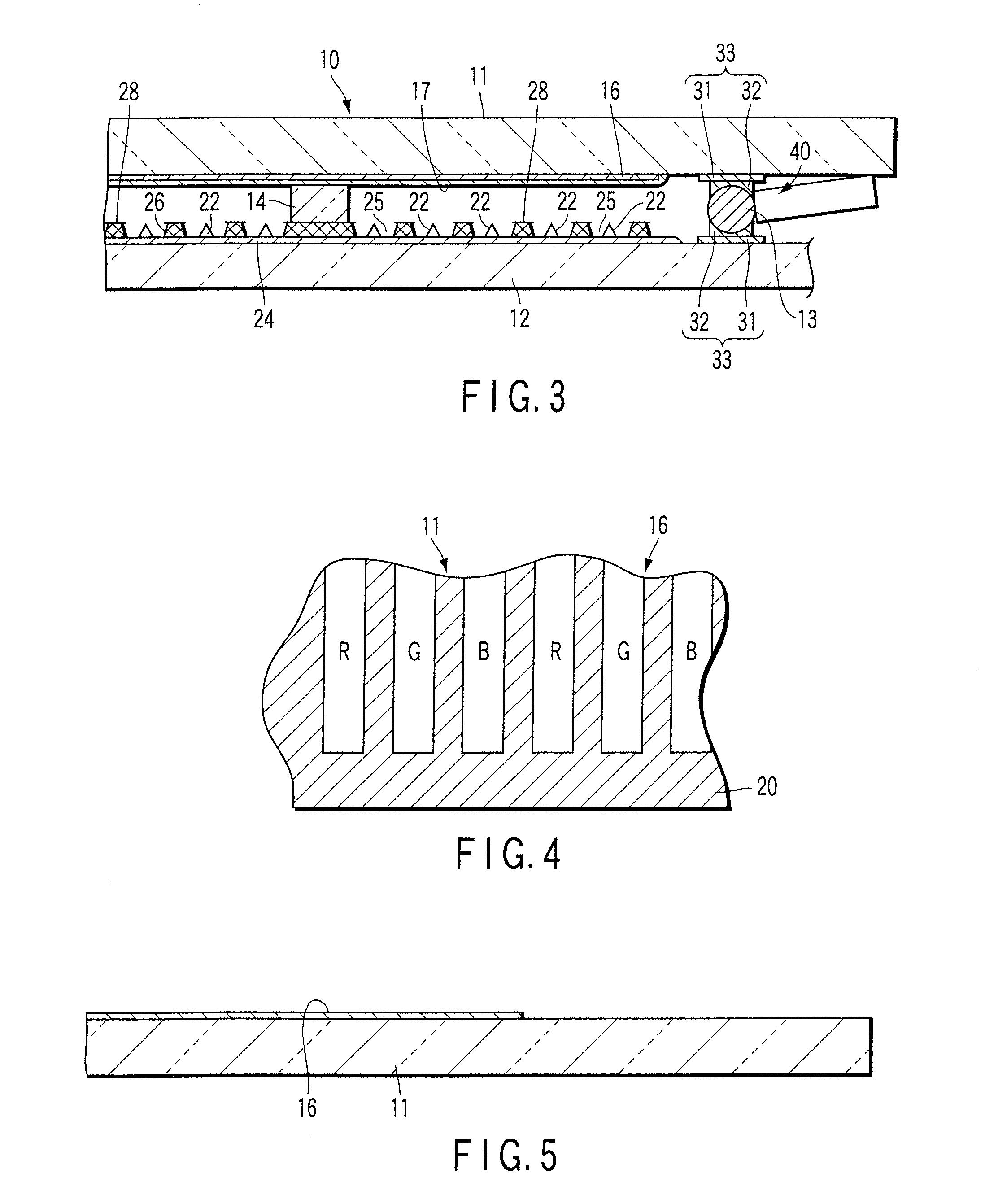
[0035] Embodiments of the present invention in which a display device according to the present invention is applied to an FED with reference to the accompanying drawings.

[0036] As shown in FIGS. 1 to 3, the FED includes insulating substrates of a front substrate 11 and a back substrate 12, which are formed with rectangular glass plates. Those substrates are oppositely arranged with a gap of 1 to 2 mm formed therebetween. The front substrate 11 and the back substrate 12 are bonded together along the peripheral portion in a state that a rectangular frame-like side wall 13 is interposed therebetween, to thereby constitute a flat, rectangular vacuum envelope 10 the inside of which is kept in a vacuum state.

[0037] The peripheral portions of the front substrate 11 and the back substrate 12 are bonded together by a sealing portion 40. More specifically, the side wall 13 functioning as a frame body is arranged between a sealing face located on an inner peripheral edge of the front substra...


PUM


Abstract

The present application relates to a method of manufacturing an image display device. The manufacturing method includes a step of arranging a side wall made of metal extending along an inner peripheral edge of a front substrate or a back substrate on the inner peripheral edge in a state that the side wall is spaced from a sealing layer, a step of melting or softening the sealing layer by heating the sealing layer and the side wall, and at the same time, discharging gas from the from the side wall, and a step of pressing the side wall against the sealing layer to be bonded thereto by moving the front substrate and the back substrate in a direction such that the substrates are close to each other.

Description

CROSS-REFERENCE TO RELATED APPLICATIONS [0001] This is a Continuation Application of PCT Application No. PCT / JP2005 / 007726, filed Apr. 22, 2005, which was published under PCT Article 21(2) in Japanese. [0002] This application is based upon and claims the benefit of priority from prior Japanese Patent Application No. 2004-141130, filed May 11, 2004, the entire contents of which are incorporated herein by reference.BACKGROUND OF THE INVENTION [0003] 1. Field of the Invention [0004] The present invention relates to a method of manufacturing an image display device of a flat shape, which has oppositely arranged substrates. [0005] 2. Description of the Related Art [0006] Recently, various types of image display devices have been developed as the next generation image display device, light in weight and flat in shape, which will supersede a cathode ray tube (referred to as a CRT). Examples of those image display devices are a liquid crystal display (referred to as an LCD) which controls l...

Claims


Application Information

Patent Timeline
IPC IPC(8): H01L21/44H01J9/26H01J29/86H01J31/12
CPCH01J9/261H01J9/241H01J9/26H01J2329/941
Inventor WADA, HIROYUKIYAMADA, AKIYOSHI
Owner KK TOSHIBA
Why Eureka
Eureka Blog
Learn More