Display device and electronic apparatus

a technology of electronic equipment and display device, which is applied in the direction of non-linear optics, instruments, optics, etc., can solve the problems of reducing the pressing force due to the resilience toward the conductive material, the failure of the product to meet the requirements of the application, and the failure to ensure the long-term reliability of the product, so as to prevent the occurrence of defective continuity resulting from the separation between the substrate and the conductive material. , the effect of long-term reliability

Inactive Publication Date: 2007-04-19
SEIKO EPSON CORP
View PDF4 Cites 1 Cited by
  • Summary
  • Abstract
  • Description
  • Claims
  • Application Information

AI Technical Summary

Benefits of technology

[0009] An advantage of the invention is that it provides a display device in which occurrence of defective continuity resulting from separation between a substrate and a conductive material is prevented and long-term reliability is ensured, and an electronic apparatus including the display device.
[0010] According to an aspect of the invention, a display device includes a first substrate, a second substrate, and microcapsules sandwiched between the first substrate and the second substrate, the microcapsules constituting a display area, the microcapsules encapsulating a display material whose optical properties change in response to electrical stimulation, wherein a conductive material for conducting between the substrates is provided between the first substrate and the second substrate to constitute a vertically conducting portion, and wherein the thickness of the conductive material is set such that the distance between the first substrate and the second substrate at the vertically conducting portion is larger than the distance between the first substrate and the second substrate in the display area.
[0011] In the display device, the thickness of the conductive material is set such that the distance between the first substrate and the second substrate at the vertically conducting portion is larger than the distance between the first substrate and the second substrate in the display area. Thus, the first substrate and / or the second substrate are / is warped outward at the vertically conducting portion and elastically deformed with respect to the display area Consequently, the first substrate and / or the second substrate, due to the resilience thereof, exert / exerts force that acts inward, i.e., force that presses the conductive material side, in particular at the vertically conducting portion. Since the first substrate and / or the second substrate always press / presses the conductive material side in such a manner, for example, even if a reliability test, such as a high-temperature preservation test or a temperature cycling test, is performed, separation between the first substrate or the second substrate and the conductive material is prevented, and thus long-term reliability as a product is ensured.
[0012] In the display device, preferably, the thickness of the conductive material is set such that the distance between the first substrate and the second substrate at the vertically conducting portion is larger than the distance between the first substrate and the second substrate in the display area by a range of 10 to 200 μm. If the difference of the distance between the substrates at the vertically conducting portion is less than 10 μm, the pressing force due to the resilience toward the conductive material is decreased, and there is a possibility that separation may occur in the reliability test. If the difference exceeds 200 μm, there is a possibility that, because of the change with time for a long period of time, the microcapsules lying in the vicinity of the vertically conducting portion may be separated from the substrates, resulting in defective display. Consequently, by specifying the range of 10 to 200 μm, both long-term reliability on defective continuity and long-term reliability on defective display can be ensured.
[0013] Furthermore, in the display device, preferably, the vertically conducting portion is disposed at the perimeter of each of the first substrate and the second substrate. In such a manner, since the resilience acts more strongly, the force that presses the conductive material side is more satisfactorily exerted.
[0014] Furthermore, in the display device, preferably, an adhesive layer which bonds the first substrate to the second substrate is provided between the first substrate and the second substrate at a position different from that of the vertically conducting portion and from that of the display area. In such a manner, the first substrate and the second substrate are bonded to each other more strongly, and thus separation between each substrate and the conductive material can be prevented.

Problems solved by technology

However, in the display device having the structure described above, when reliability tests, such as a high-temperature preservation test and a temperature cycling test, are performed, in some cases, separation may occur between the transparent substrate or the substrate and the conductive material due to thermal expansion and thermal shrinkage of the resin in the conductive material, resulting in defective continuity.
When defective continuity occurs in such reliability tests, it is expected that long-term reliability may not be ensured when the product is in the market.
If the difference of the distance between the substrates at the vertically conducting portion is less than 10 μm, the pressing force due to the resilience toward the conductive material is decreased, and there is a possibility that separation may occur in the reliability test.
If the difference exceeds 200 μm, there is a possibility that, because of the change with time for a long period of time, the microcapsules lying in the vicinity of the vertically conducting portion may be separated from the substrates, resulting in defective display.

Method used


Image

  • Display device and electronic apparatus
  • Display device and electronic apparatus
  • Display device and electronic apparatus

Examples


Embodiment Construction

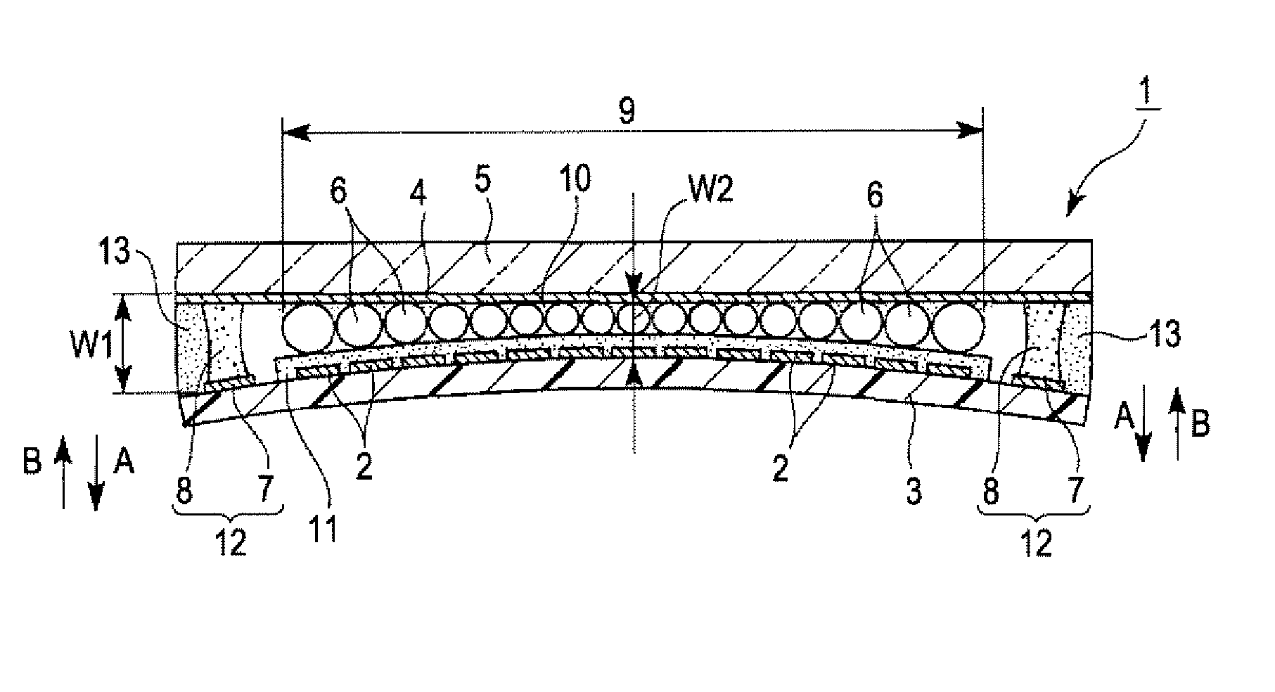
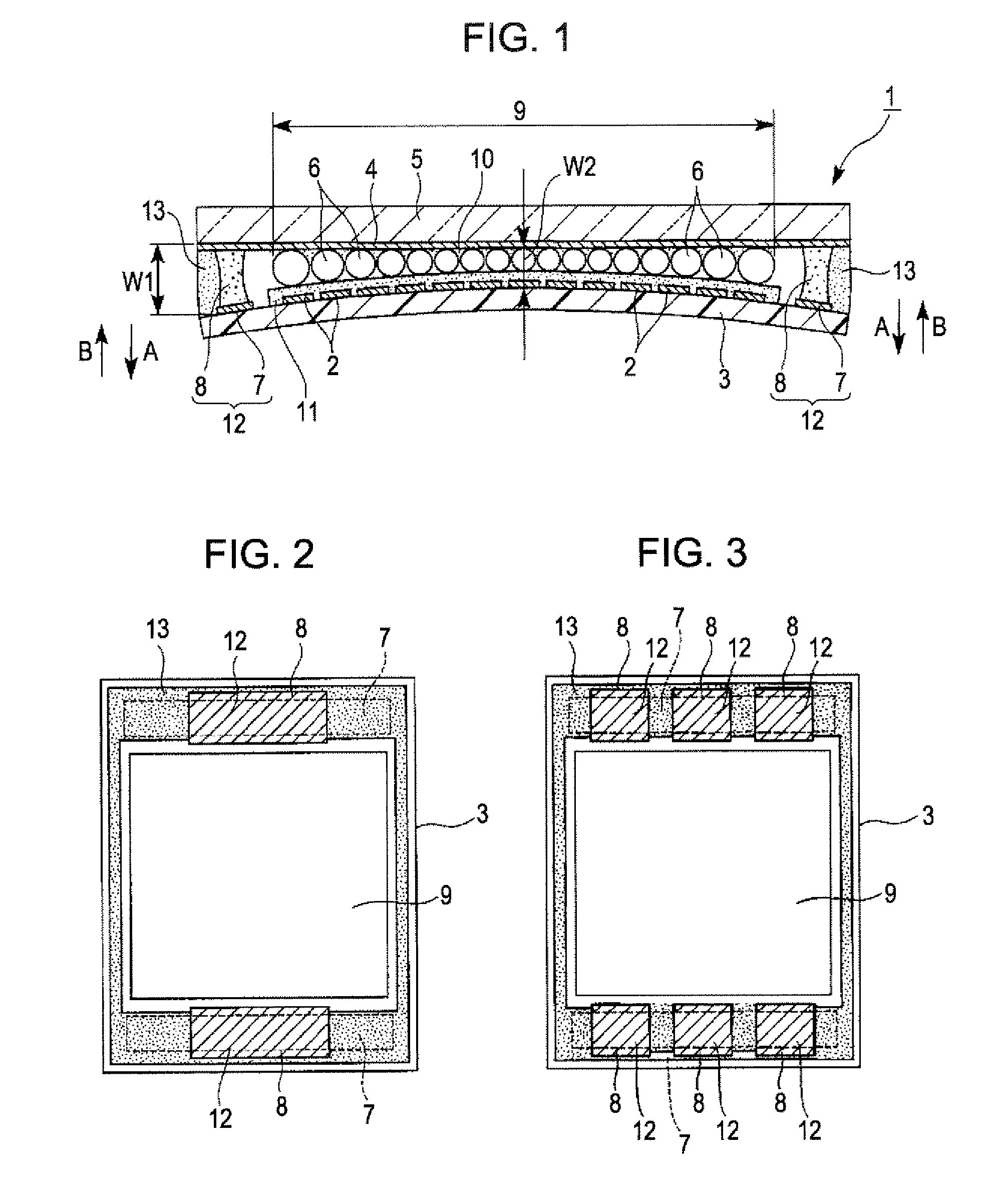
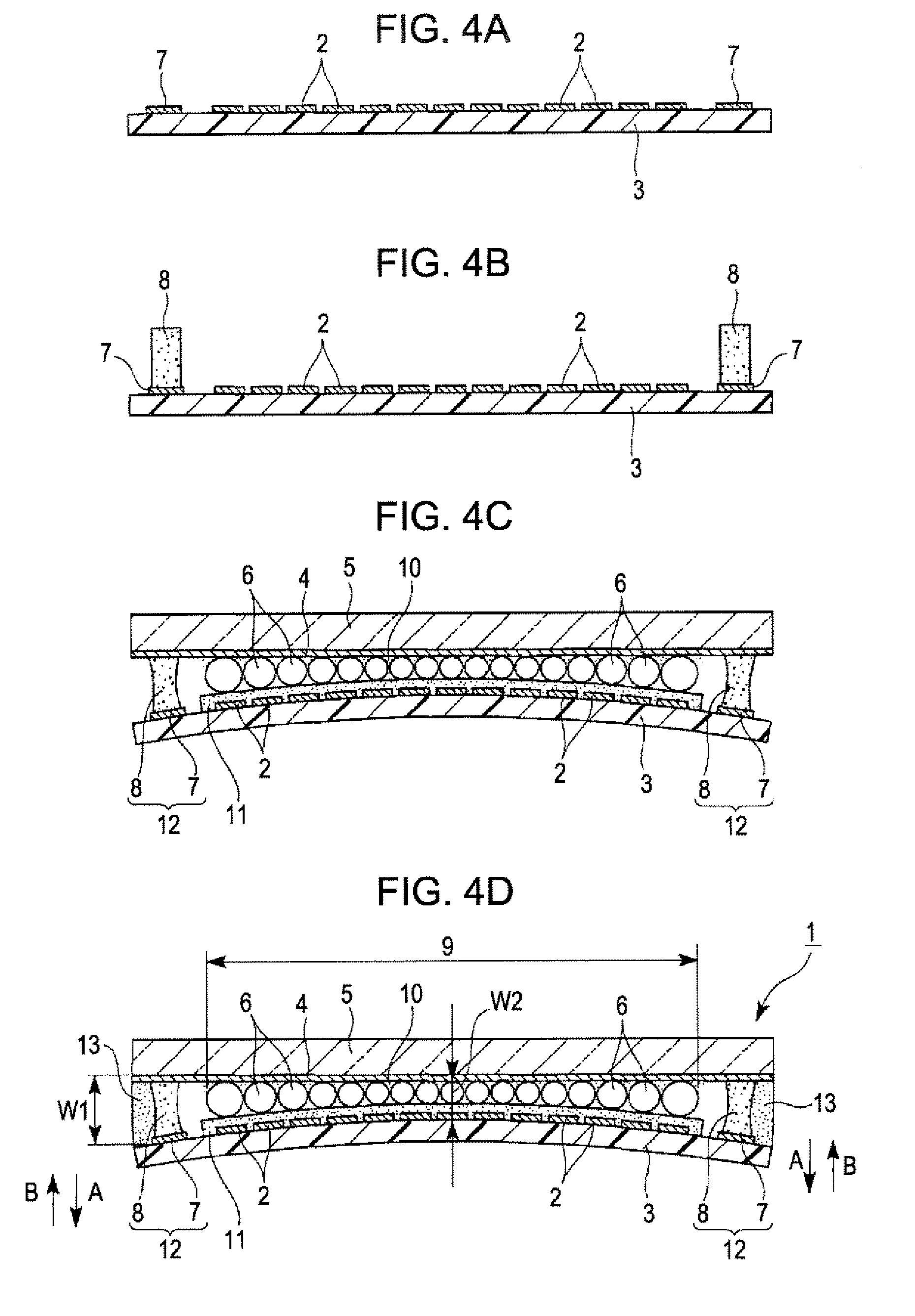
[0031] The invention will be described in detail below. FIG. 1 is a schematic diagram showing a display device according to an embodiment of the invention. In FIG. 1, reference numeral 1 represents a display device. Note that, in FIGS. 1 and 4A to 4D, in order to facilitate understanding of the characteristic parts of the invention, the device is schematically shown with the size and shape being extremely changed from the actual size and shape. In particular, although microcapsules in the center and microcapsules at both ends are shown to have different diameters, all the microcapsules are actually formed so as to have substantially the same diameter.

[0032] The display device 1 includes a first substrate 3 provided with a plurality of pixel electrodes 2 and a second substrate 5 provided with a common electrode (counter electrode) 4. Microcapsules 6 encapsulating a display material are sandwiched between the first substrate 3 and the second substrate 5. Such a display device 1 can b...


PUM

PropertyMeasurementUnit
thicknessaaaaaaaaaa
distanceaaaaaaaaaa
thicknessaaaaaaaaaa

Abstract

A display device includes a first substrate, a second substrate, and microcapsules sandwiched between the first substrate and the second substrate, the microcapsules constituting a display area, the microcapsules encapsulating a display material whose optical properties change in response to electrical stimulation. A conductive material for conducting between the substrates is provided between the first substrate and the second substrate to constitute a vertically conducting portion. The thickness of the conductive material is set such that the distance between the first substrate and the second substrate at the vertically conducting portion is larger than the distance between the first substrate and the second substrate in the display area.

Description

BACKGROUND [0001] 1. Technical Field [0002] The present invention relates to a display device provided with microcapsules and an electronic apparatus including the display device. [0003] 2. Related Art [0004] Hitherto, electrophoretic display devices, each of which includes an electrophoretic dispersion liquid containing a liquid-phase dispersion medium and electrophoretic particles and utilizes the phenomenon in that the distribution state of the electrophoretic particles changes in the presence of an applied electric field, thus changing the optical properties of the electrophoretic dispersion liquid, have been known (for example, refer to Japanese Unexamined Patent Application Publication No. 9-185087 [Patent Document 1]). In such electrophoretic display devices, since a backlight is not required, the cost can be reduced and the thickness can be decreased. Moreover, the electrophoretic display devices provide a wide angle of view and a high contrast, and also have memory effects ...

Claims


Application Information

Patent Timeline
Patent Type & Authority Applications(United States)
IPC IPC(8): G02F1/1333G02F1/167G02F1/1675
CPCG02F1/1339G02F1/167G02F2001/133388G02F1/1675G02F1/133388
Inventor UCHIDA, MASAMI
Owner SEIKO EPSON CORP
Why Eureka
Try Eureka