Semiconductor memory and driving method for the same
- Summary
- Abstract
- Description
- Claims
- Application Information
AI Technical Summary
Benefits of technology
Problems solved by technology
Method used
Image
Examples
embodiment 1
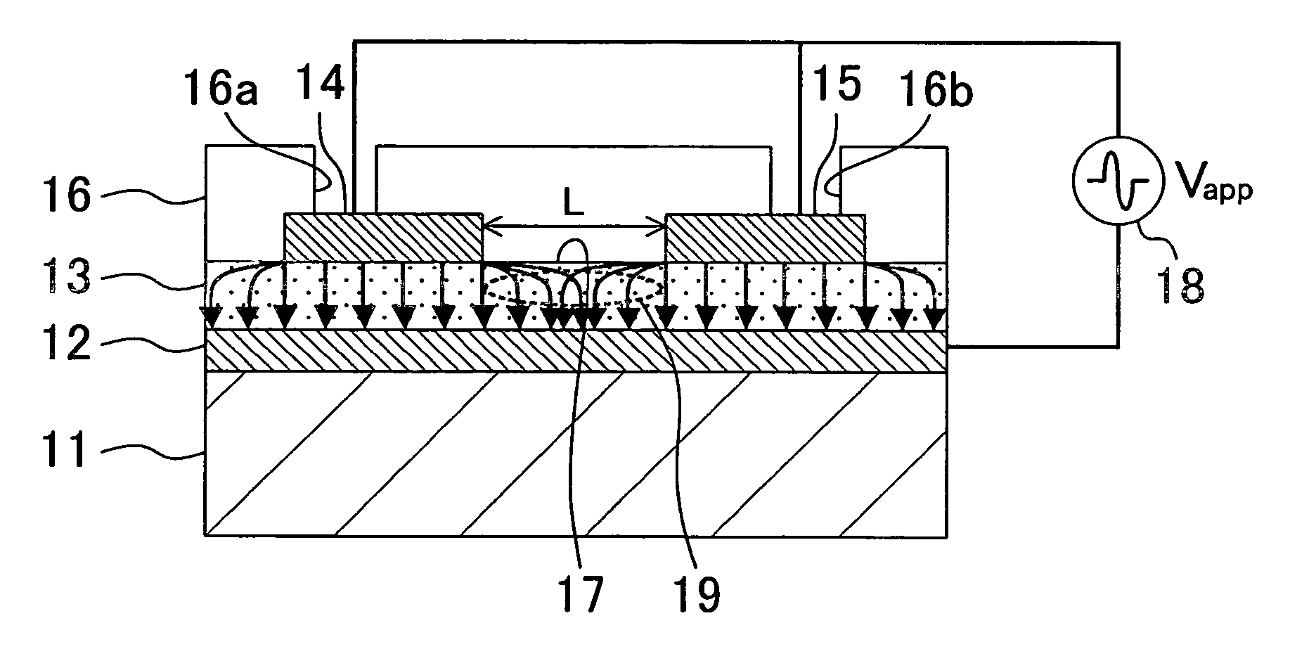
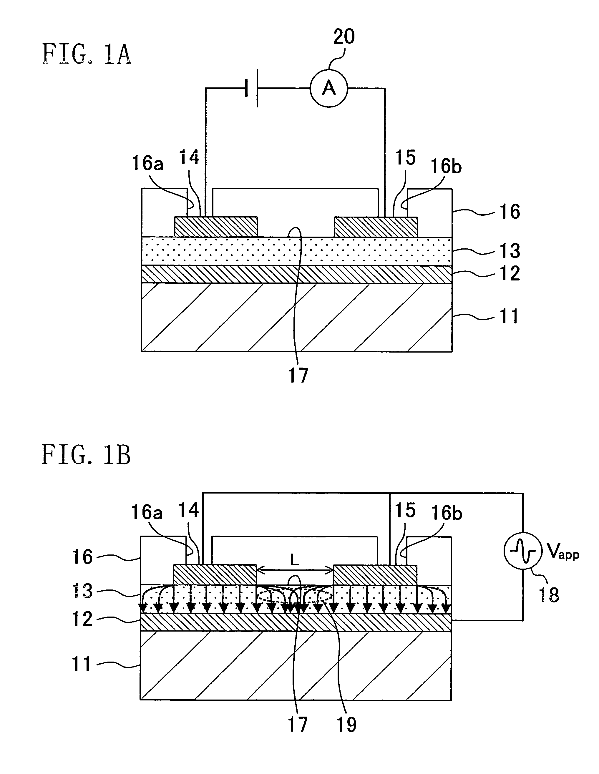
[0061] A semiconductor memory and a method for fabricating the same according to Embodiment 1 of the invention will now be described with reference to FIGS. 1A and 1B.
[0062]FIGS. 1A and 1B are cross-sectional views for showing the structural concept of the semiconductor memory of Embodiment 1 of the invention, and FIG. 1A also shows a configuration for reading data and FIG. 1B also shows a configuration for writing data and a conceptual diagram of electric flux lines caused in a ferroelectric film.
[0063]—Structure of Semiconductor Memory of Embodiment 1
[0064] As shown in FIGS. 1A and 1B, a lower electrode 12 made of a conducting film and a ferroelectric film 13 are stacked in this order in the upward direction on a substrate 11. A source electrode 14 and a drain electrode 15 both made of a conducting film and spaced from each other are formed on the ferroelectric film 13. Also, an insulating film 16 is formed on the ferroelectric film 13 so as to cover the source electrode 14 and...
embodiment 2
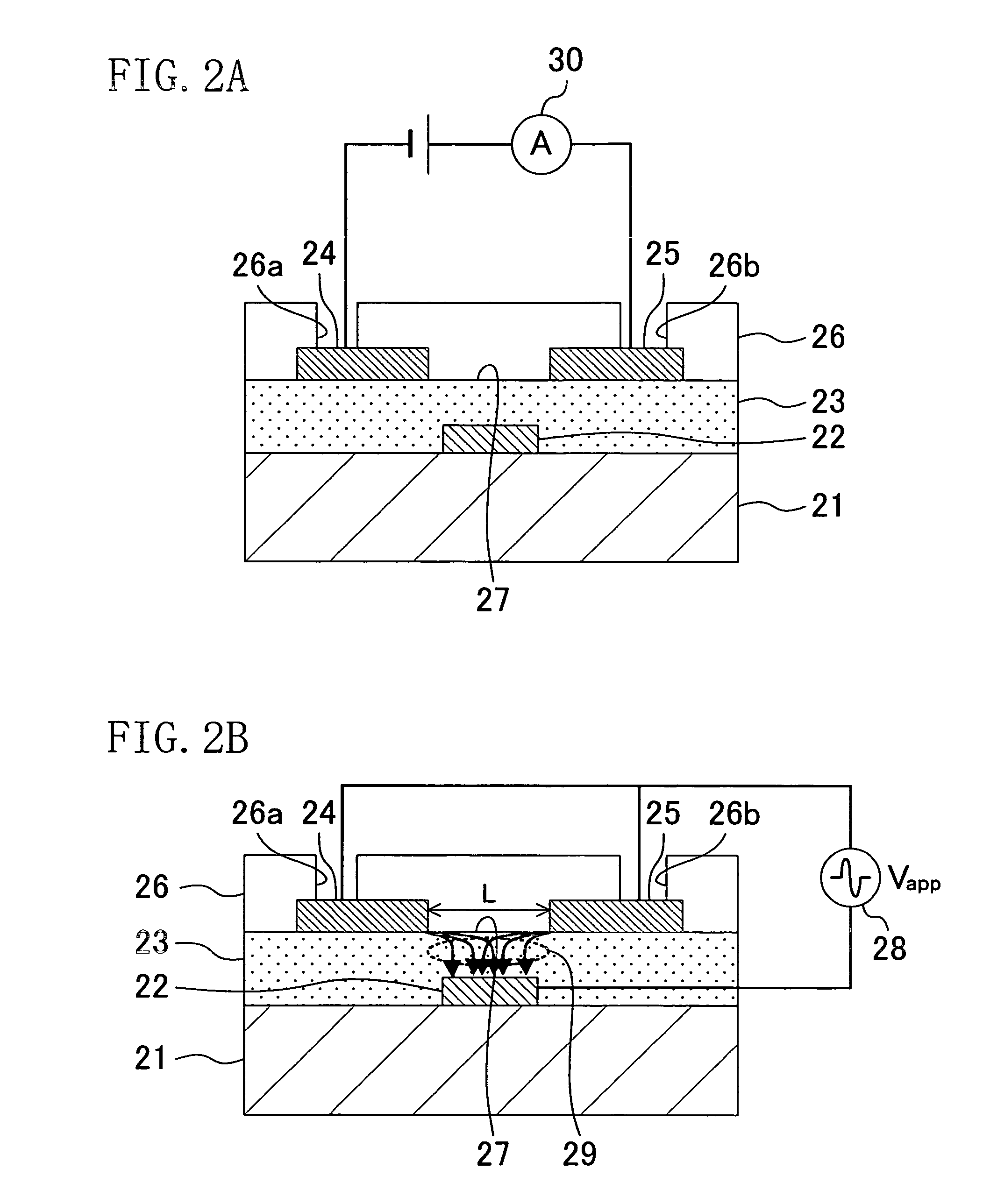
[0083] A semiconductor memory and a method for fabricating the same according to Embodiment 2 of the invention will now be described with reference to FIGS. 2A and 2B.
[0084]FIGS. 2A and 2B are cross-sectional views for showing the structural concept of the semiconductor memory of Embodiment 2 of the invention, and FIG. 2A also shows a configuration for reading data and FIG. 2B also shows a configuration for writing data and a conceptual diagram of electric flux lines caused in a ferroelectric film.
[0085]—Structure of Semiconductor Memory of Embodiment 2
[0086] As shown in FIGS. 2A and 2B, a lower electrode 22 made of a conducting film is formed on a substrate 21 and a ferroelectric film 23 is formed so as to cover the lower electrode 22. A source electrode 24 and a drain electrode 25 both made of a conducting film and spaced from each other are formed on the ferroelectric film 23. Also, an insulating film 26 is formed on the ferroelectric film 23 so as to cover the source electrod...
embodiment 3
[0098] A semiconductor memory and a method for fabricating the same according to Embodiment 3 of the invention will now be described with reference to FIGS. 3A and 3B.
[0099]FIGS. 3A and 3B are cross-sectional views for showing the structural concept of the semiconductor memory of Embodiment 3 of the invention, and FIG. 3A also shows a configuration for reading data and FIG. 3B also shows a configuration for writing data and a conceptual diagram of electric flux lines caused in a ferroelectric film.
[0100]—Structure of Semiconductor Memory of Embodiment 3
[0101] As shown in FIGS. 3A and 3B, lower electrodes 32a and 32b made of a conducting film and spaced from each other are formed on a substrate 31 and a ferroelectric film 33 is formed so as to cover the lower electrodes 32a and 32b. A source electrode 34 and a drain electrode 35 both made of a conducting film and spaced from each other are formed on the ferroelectric film 33. Also, an insulating film 36 is formed on the ferroelect...
PUM
 Abstract
Description
Claims
Application Information
 - R&D
- Intellectual Property
- Life Sciences
- Materials
- Tech Scout
- Unparalleled Data Quality
- Higher Quality Content
- 60% Fewer Hallucinations
Browse by: Latest US Patents, China's latest patents, Technical Efficacy Thesaurus, Application Domain, Technology Topic, Popular Technical Reports.
© 2025 PatSnap. All rights reserved.Legal|Privacy policy|Modern Slavery Act Transparency Statement|Sitemap|About US| Contact US: help@patsnap.com


