Terahertz radiating device based on semiconductor coupled quantum wells

a quantum well and terahertz radiation technology, applied in semiconductor devices, lasers, semiconductor lasers, etc., can solve the problems of low average power, low ionizing capability, and limited recent achievements in both directions, so as to improve radiative characteristics, suppress optical phonon scattering, and improve radiative characteristics

Inactive Publication Date: 2007-03-08
YISSUM RES DEV CO OF THE HEBREWUNIVERSITY OF JERUSALEM LTD
View PDF16 Cites 7 Cited by
  • Summary
  • Abstract
  • Description
  • Claims
  • Application Information

AI Technical Summary

Benefits of technology

[0027] Furthermore, the semiconductor device according to the present invention can demonstrate improved radiative characteristics, because the Auger recombination is suppressed owing to the rather effective nearly static screening of the Coulomb interaction contrary to the much less effective dynamic screening in the infrared and optical wavelength range. Likewise, the radiative characteristics can be improved because the optical phonon scattering can be suppressed when the radiated frequency is lower than the typical radiated frequency of optical phonons.
[0028] Moreover, the semiconductor device according to the present invention is of a durable and reliable construction, may be easily and efficiently manufactured and marketed, and may have low manufacturing cost.

Problems solved by technology

However, having low average power, i.e. relatively low ionizing capability, T-rays are particularly attractive for medical applications where it is important to avoid damaging a biological sample.
Recent achievements in both fields mentioned above are rather remarkable, but still limited.
The key reason for this limitation is a lack of reliable THz sources and detectors, especially when compared with the neighboring frequency ranges of microwaves and infrared radiation.

Method used


Image

  • Terahertz radiating device based on semiconductor coupled quantum wells
  • Terahertz radiating device based on semiconductor coupled quantum wells
  • Terahertz radiating device based on semiconductor coupled quantum wells

Examples


Embodiment Construction

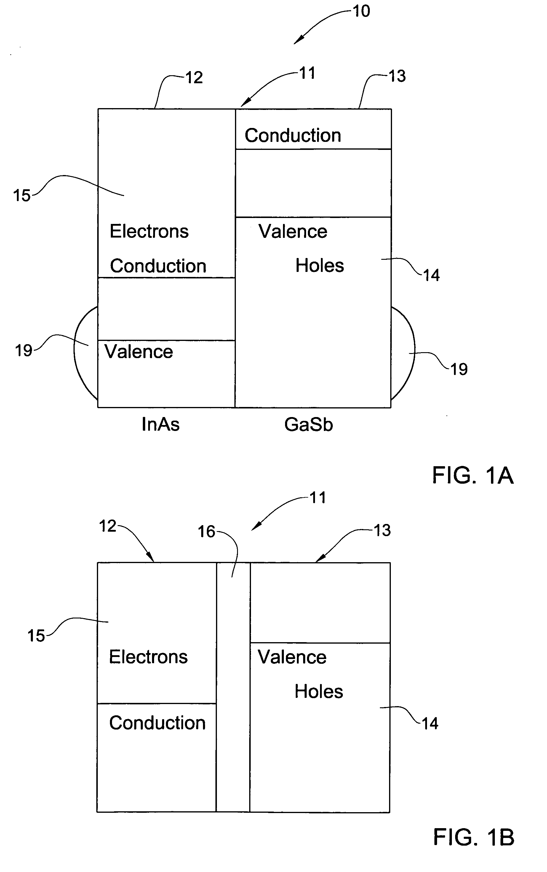
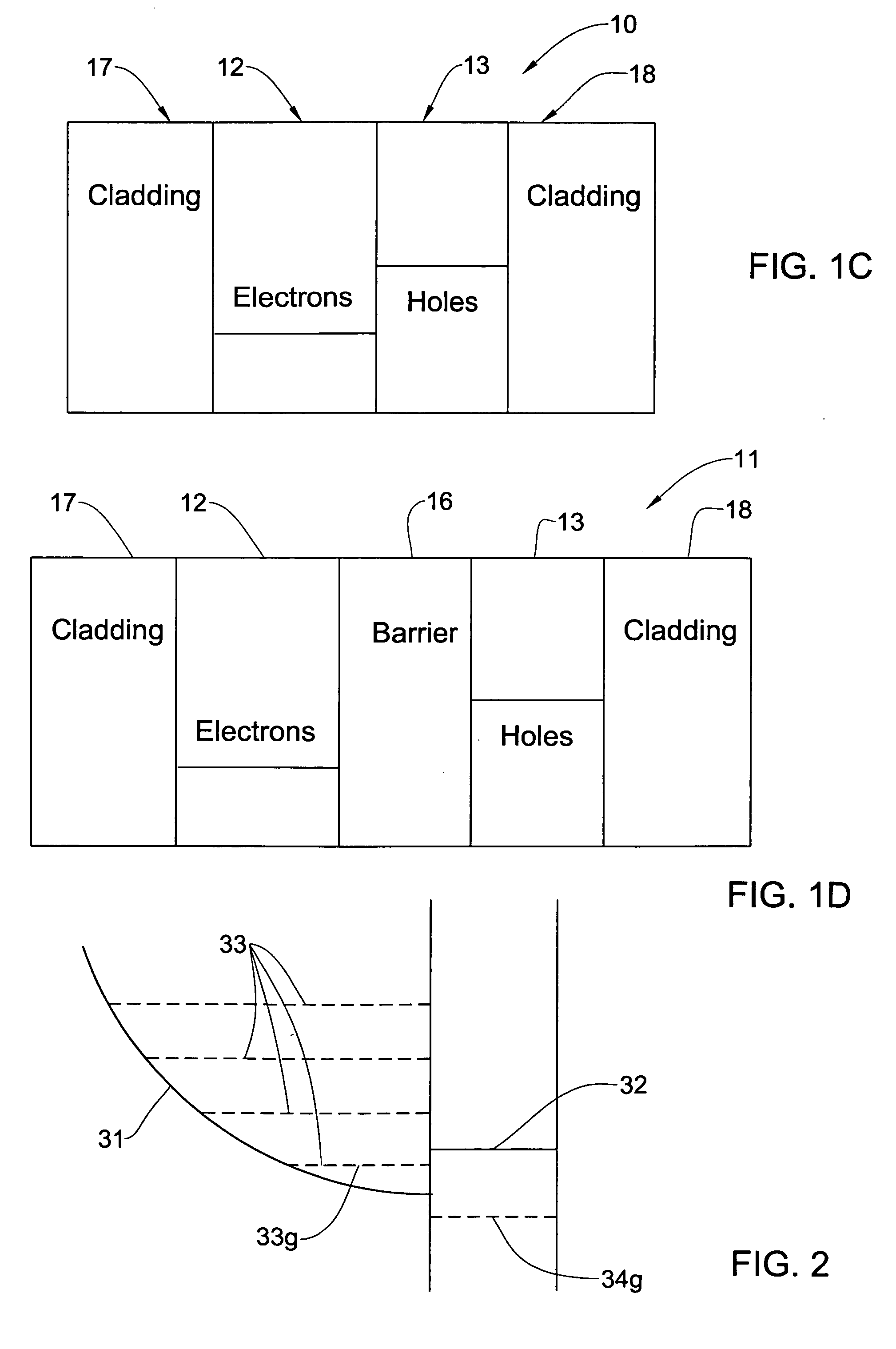
[0062] The principles and operation of a device according to the present invention may be better understood with reference to the drawings and the accompanying description, it being understood that these drawings and examples in the description are given for illustrative purposes only and are not meant to be limiting. Dimensions of layers and regions may be exaggerated for clarity. The same reference numerals will be utilized for identifying those components which are common in all the examples of the invention.

[0063] Referring to FIG. 1A, there is illustrated a schematic cross-sectional view of an exemplary semiconductor device 10 operable in terahertz (THz) spectral range, according to the present invention. It should be noted that this figure is not to scale, and is not in proportion, for purposes of clarity. The device 10 may for example be a source (emitter) of THz radiation.

[0064] The semiconductor device 10 comprises a heterostructure 11 including a first semiconductor laye...


PUM


Abstract

A method is presented for fabricating a semiconductor device operable to generate a THz spectral range radiation in response to an external field. According to this method, a heterostructure is formed from selected layers. The layers include at least first and second semiconductor layers made of materials having a certain initial overlap between the valence band of the second layer material and the conduction band of the first layer material. The heterostructure layers are arranged with a selected layout providing a quantum mechanical coupling between an electron quantum well (EQW) in said first layer and a hole quantum well (HQW) in said second layer. The layout is selected so as to define a predetermined arrangement of a plurality of energy subbands and a predetermined dispersion of these subbands to define a desired effective overlap between the energy subbands of said conduction and valence bands. This enables the device operation for generation of the THz spectral range radiation originating from multiple radiative transitions of non-equilibrium carriers including at least one transition from transitions between the following: energy subbands of the EQW, energy subbands of the HQW, and ground energy electron subband of the EQW and ground energy hole subband of the HQW.

Description

FIELD OF THE INVENTION [0001] The present invention relates generally to terahertz radiating semiconductor devices, and more particularly to a quantum well oscillator operating in a terahertz region. BACKGROUND OF THE INVENTION [0002] A terahertz region of the spectrum of electromagnetic radiation (T-Rays or THz) is located between the most long wavelength “optical” part of the spectrum, i.e. the infra-red light, and the most short wavelength part of the “radio” spectrum, known as microwaves. The terahertz spectral region thus encompasses the frequencies in the range of about 0.1 through 20 THz or the wavelengths in the range of about 15 μm through 3 mm, although it should be appreciated that these limits are indicative rather than absolute. [0003] The terahertz spectral range has an extreme importance owing to the variety of applications where it can be utilized. One important application of the terahertz spectral range is related to various imaging techniques (medical imaging, tec...

Claims


Application Information

Patent Timeline
Patent Type & Authority Applications(United States)
IPC IPC(8): H01L21/00H01L29/06H01S5/34
CPCB82Y20/00H01S5/34H01S2302/02H01S5/3425H01S5/3407
Inventor LAIKHTMAN, BORISSHVARTSMAN, LEONID D.
Owner YISSUM RES DEV CO OF THE HEBREWUNIVERSITY OF JERUSALEM LTD
Why Eureka
Try Eureka