Structure and assembly method of integrated circuit package

a technology of integrated circuits and assembly methods, which is applied in the direction of electrical equipment, semiconductor devices, semiconductor/solid-state device details, etc., can solve the problems of large amount of trace routing between solder balls and bonding fingers, easy shorting, and large density of bonding wires, so as to reduce cost, prevent shorting, and simplify trace routing

Inactive Publication Date: 2006-10-12
SILICON INTEGRATED SYSTEMS
View PDF6 Cites 14 Cited by
  • Summary
  • Abstract
  • Description
  • Claims
  • Application Information

AI Technical Summary

Benefits of technology

[0008] In view of the foregoing, it is an object of the present invention to provide an universal substrate that is adaptable for packaging most types of the dies. The use of the substrate also simplifies the trace routing, reduces the cost, and prevents shorting.
[0009] Another object of the present invention is to provide a packaging structure with effective electrical and magnetic shielding. The packaging structure effectively distributes the grounding, and therefore simplifies the circuit layout and decreases the cost.
[0010] According to the object, one embodiment of the present invention provides a packaging structure and an assembly method thereof. A substrate includes pads (such as bonding fingers), conductive vias formed below or beside the pads, and solder balls. After a die is mounted on the substrate, insulator-coated wires are bonded. Accordingly, the present invention can be universally adaptable for packaging dies, simplify the circuit layout, and prevent shorting. Thereafter, conductively filled material is filled onto the die and the substrate, thereby effectively providing electrical and magnetic shielding.

Problems solved by technology

As the packaging structures get smaller and its circuitry more complex, the density of the bonding wires greatly increases.
Conventional bonding wires are non-insulating to each other, so that they are easily shorted.
Furthermore, the communication paths between the solder balls and the bonding fingers require large amount of trace routing on both sides of the substrate.
In other words, a packaging structure designed for one die is difficult to be adapted to other dies.
The custom-made design not only increases stockpiles, but also prolongs time to market or time to be certified.
Further, the requirement of inserting shielding wires among the bonding wires makes the process more difficult and costs more.
Even the shielding wires can shield off undesired electrical effect, they can not help prevent undesired magnetic effect.

Method used


Image

  • Structure and assembly method of integrated circuit package
  • Structure and assembly method of integrated circuit package
  • Structure and assembly method of integrated circuit package

Examples


second embodiment

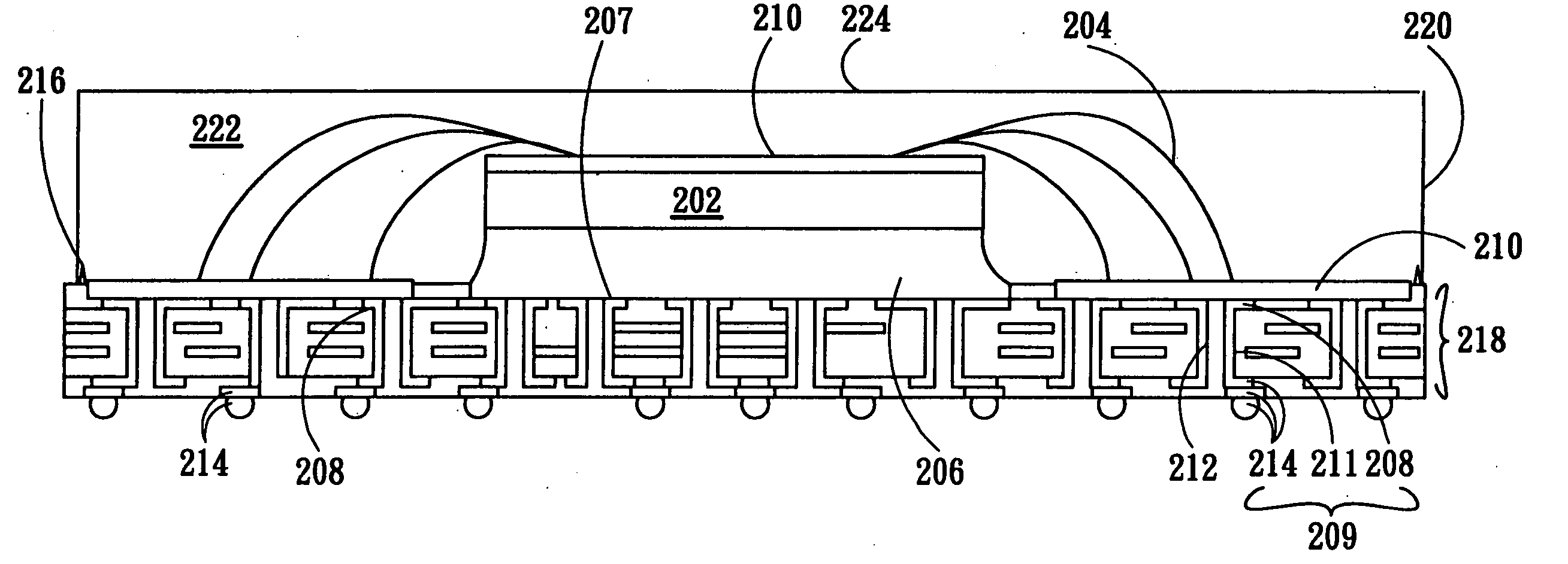
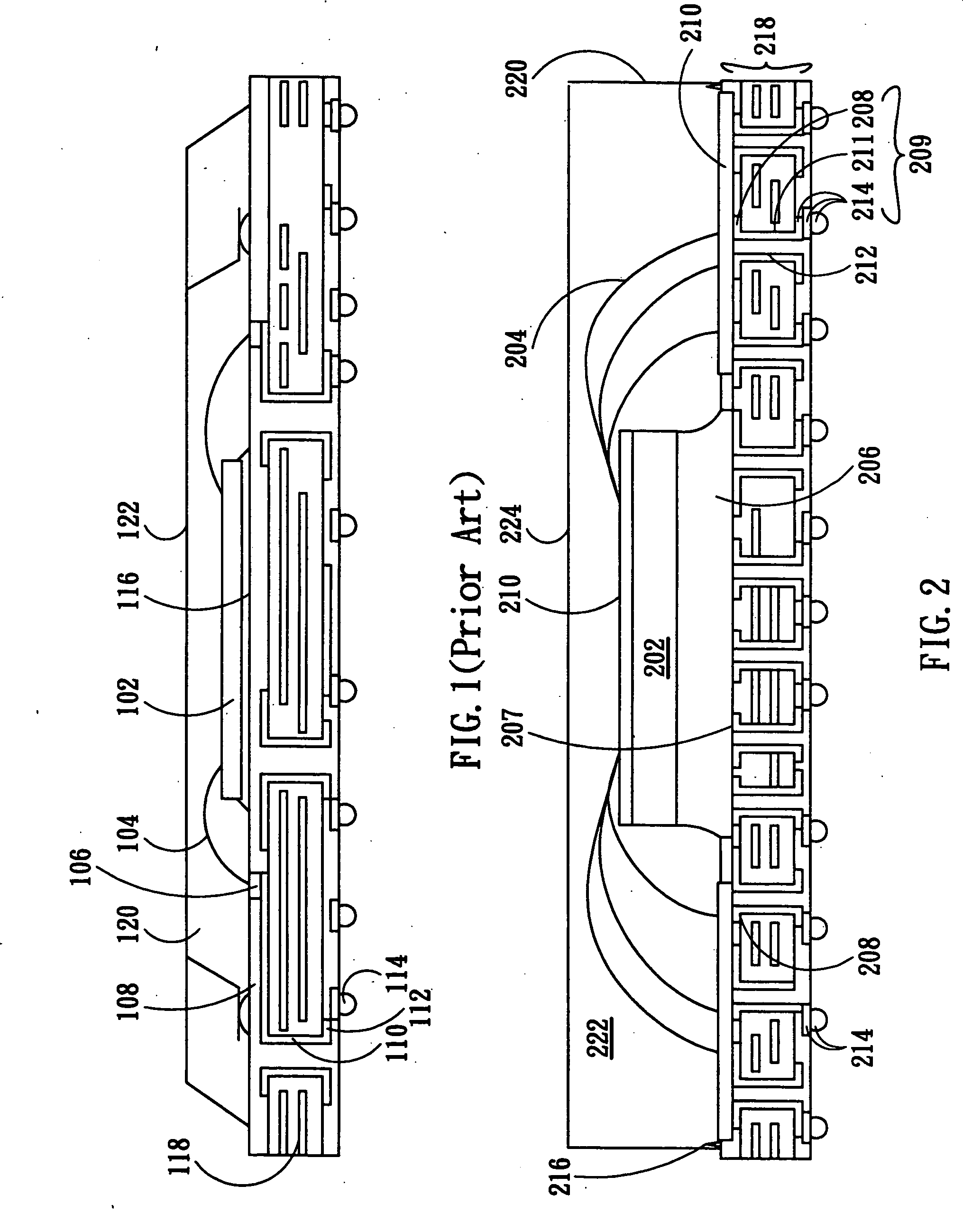
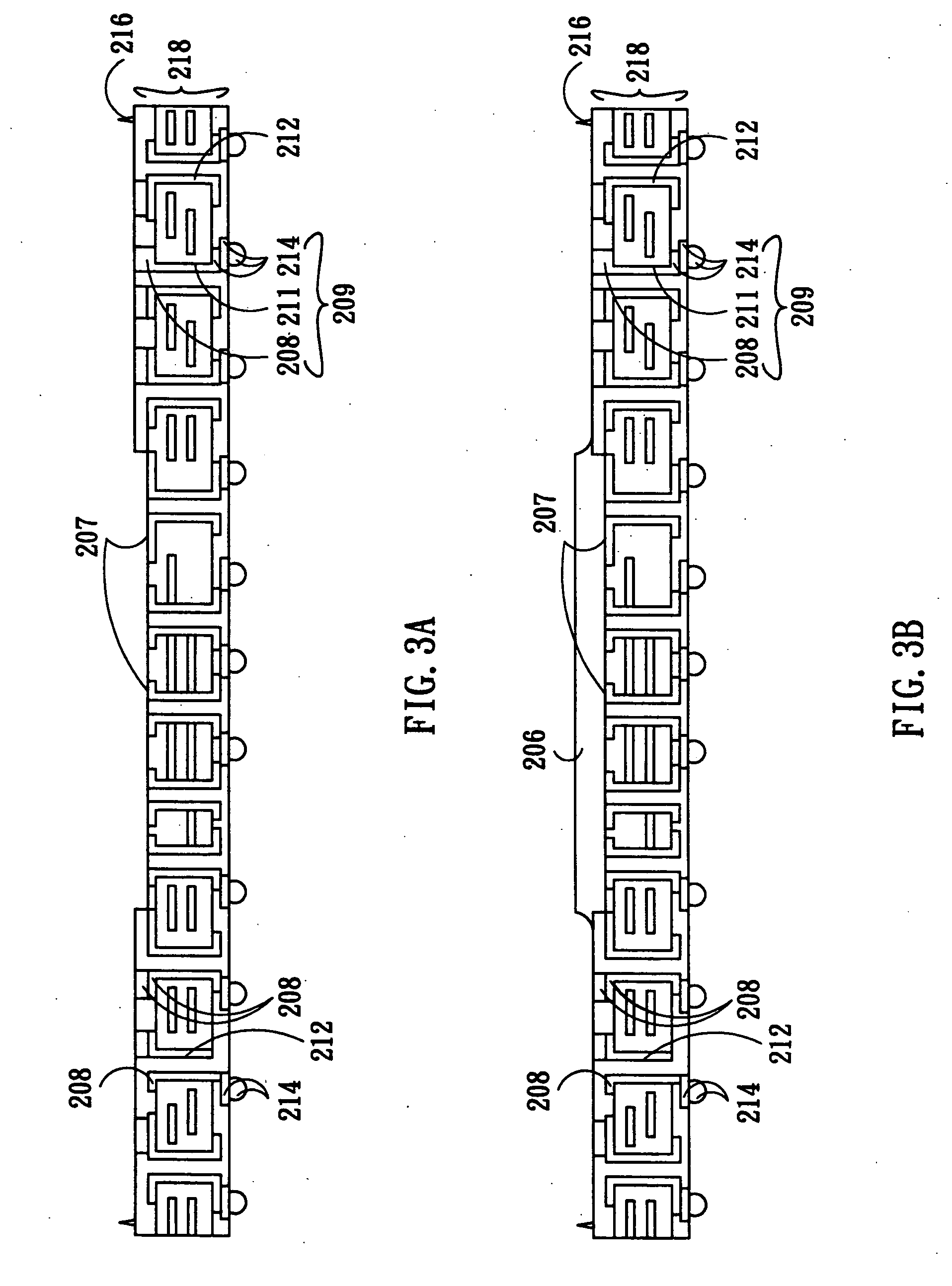
[0038]FIG. 4 is a cross-sectional view illustrating a packaging structure according to the present invention. At least one leading conductor 205a has one end connected to the ground pad of the die 202, and has the other end exposed and floated over the substrate 218. The exposed end of the leading conductor 205a electrically connects to the conductively filled material 222. Accordingly, the die 202 is grounded through the die-attach material 206 and the ground openings 207. As the leading conductor 205a is formed near the conductive wires 204, the generated heat from the die 202 can be substantially dissipated through the conductive wires 204. Besides, the stop element 216 (FIG. 2) is not used to confine the formation of the insulating layer 210 in this embodiment.

third embodiment

[0039]FIG. 5 is a cross-sectional view illustrating a packaging structure according to the present invention. At least one leading conductor 205b has one end connected to the first conductive structure 208 of the substrate 218, and has the other end exposed and floated over the substrate 218. The exposed end of the leading conductor 205b electrically connects to the conductively filled material 222. The conductively filled material 222 and the second conductive structure 214b together are therefore grounded. The object of electrical shielding can be achieved by using either conductive die-attach material 206 or non-conductive die-attach material 206.

fourth embodiment

[0040]FIG. 6A is a cross-sectional view illustrating a packaging structure according to the present invention. In this embodiment, a leading conductor 205a having one end connected to the ground pad of the die 202 and having the other end exposed and floated over the substrate 218 is used; moreover, another leading conductor 205b having one end connected to the first conductive structure 208 and having the other end exposed and floated over the substrate 218 is also used. The exposed ends of the leading conductor 205a and the leading conductor 205b electrically connect to the conductively filled material 222, and are accordingly grounded with the conductively filled material 222. Therefore, a return path between the substrate 218 and the die 202 is established to substantially shield the electrical effect. FIG. 6B shows an alternative embodiment in which at least one bare (or non-coated) leading conductor 205c is used. The bare leading conductor 205c not only connects between the pa...


PUM


Abstract

A packaging structure and an assembly method are disclosed. A packaging structure includes a substrate, a die, conductive wires, and conductively filled material. The substrate includes a conductive structure, and the conductive wires are insulator-coated. The die is mounted on the substrate, and the conductive wires are connected between the die and the conductive structure. The conductively filled material is formed among the conductive wires. In the assembly method, the die is firstly mounted on the substrate, followed by connecting the conductive wires between the die and the conductive structure, and finally forming the conductively filled material among the conductive wires.

Description

BACKGROUND OF THE INVENTION [0001] 1. Field of the Invention [0002] The present invention generally relates to a packaging structure and its assembly method, and more particularly to a packaging structure and an assembly method with a conductively filled material. [0003] 2. Description of the Prior Art [0004] Wire bonding is one of traditional integrated circuits packaging techniques. Signals are transmitted from the pads of die to the bonding fingers of a packaging substrate through bonding wires. The signals are further transmitted through trace routing, conductive vias, low layer circuit, and finally to solder balls. [0005]FIG. 1 is a cross-sectional view illustrating a conventional packaging structure. On the surface of the substrate 118 are bonding fingers 106, and the trace routing 108 connected to the bonding fingers 106. The trace routing 108 is further connected to the conductive vias 110, to the low layer circuit 112, and finally to the solder balls 114. The bonding finger...

Claims


Application Information

Patent Timeline
IPC IPC(8): H01L23/04H01L21/44
CPCH01L2924/1815H01L2924/0665H01L24/49H01L24/29H01L23/3128H01L23/50H01L23/552H01L23/60H01L24/32H01L24/45H01L24/48H01L24/83H01L2223/6611H01L2224/27013H01L2224/32225H01L2224/45144H01L2224/4554H01L2224/45565H01L2224/48091H01L2224/48227H01L2224/48237H01L2224/49175H01L2224/73265H01L2224/83051H01L2224/83192H01L2224/8385H01L2224/8592H01L2224/92H01L2224/92247H01L2924/01004H01L2924/01029H01L2924/01047H01L2924/01079H01L2924/01082H01L2924/07802H01L2924/0781H01L2924/14H01L2924/15153H01L2924/1517H01L2924/15311H01L2924/16152H01L2924/3025H01L2924/3511H01L2224/2919H01L2924/01006H01L2924/01033H01L2924/014H01L2924/00014H01L2924/00012H01L2924/00H01L2924/00011H01L2924/181H01L24/73H01L2224/05554H01L2924/10161H01L2224/43H01L21/54H01L23/02
Inventor LIANG, KUEI-CHENWU, CHUNG-JUFANG, CHUNG-YIN
Owner SILICON INTEGRATED SYSTEMS
Why Eureka
Try Eureka