Liquid crystal display for implmenting improved inversion driving technique

Inactive Publication Date: 2006-04-27
RENESAS ELECTRONICS CORP
View PDF9 Cites 37 Cited by
  • Summary
  • Abstract
  • Description
  • Claims
  • Application Information

AI Technical Summary

Benefits of technology

[0025] The architecture of the liquid crystal display apparatus according to the present invention effectively reduces the difference between the maximum signal level of the positive data signals and the ground level of the LCD driver, and also reduces the difference between the ground level of the LCD driver and the minimum signal level of the negative data signals, approximately down to the maximum voltages applied across the pixels, not twice of the maximum voltages. In other words, this architecture effectively reduces the power source voltages of both of the positive and negative drive circuits approximately down to the maximum voltages applied across the pixels. This effectively reduces the power consumption of the LCD driver.
[0026] Preferably, the liquid crystal display apparatus additionally includes a precharge circuitry for precharging the data lines within the LCD panel to the ground level of said LCD driver. Such architecture effectively reduces the voltage applied to the positive and negative drive circuits, and also reduces the power consumption necessary for precharging the data lines.

Problems solved by technology

Liquid crystal displays often suffer from the “burn-in” effect, which is known as a phenomenon in which applying a DC voltage to pixels within a liquid crystal display causes serious degradation of the lifetime of liquid crystal material filled in the pixels.
One issue of conventional common constant driving techniques is that drive circuits developing data signals are required to operate on a high power source voltage.
Operating drive circuits on a high power supply voltage is accompanied by two disadvantages: Firstly, circuit elements within the drive circuits are required to have a high withstand voltage, specifically, equal to or higher than twice of the maximum voltages applied to the pixels.
Another disadvantage is the increase in the power consumption.
The power consumption of the drive circuits proportionally increases as the power supply voltage, and therefore, the increase in the power supply voltage undesirably increases the power consumption.
Although reducing the power supply voltage fed to the negative drive circuits 104d down to 5 V, the architecture shown in FIG. 5 requires feeding the power supply voltage as high as 10 V. This is undesirable for reducing the power consumption.

Method used


Image

  • Liquid crystal display for implmenting improved inversion driving technique
  • Liquid crystal display for implmenting improved inversion driving technique
  • Liquid crystal display for implmenting improved inversion driving technique

Examples


first embodiment

(Structure of LCD Apparatus)

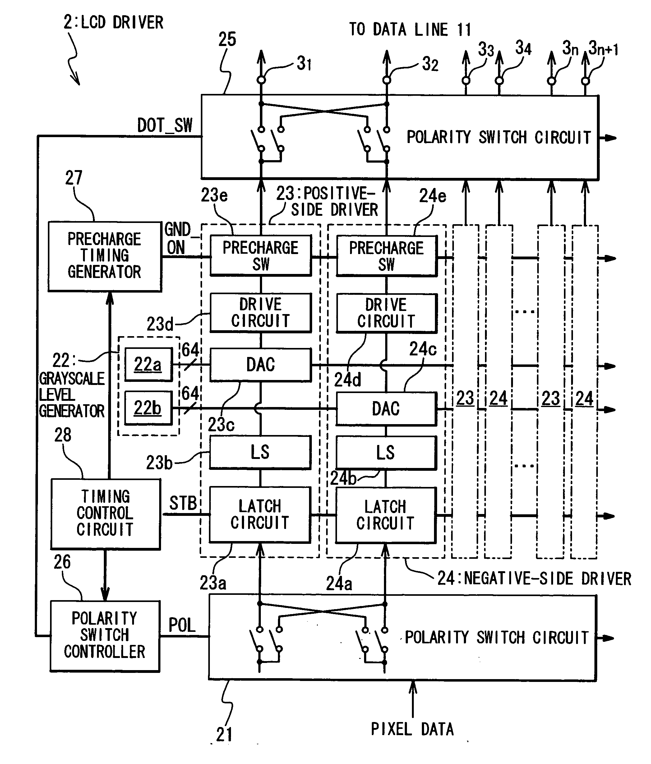
[0041]FIG. 3 is a diagram illustrating an exemplary structure of an LCD apparatus 10 in a first embodiment of the present invention. The LCD apparatus 10 is composed of an LCD panel 1, and an LCD driver 2. The LCD panel 1 is composed of data lines 11, gate lines 12, and pixels 13 arranged at respective intersections of the data lines 11 and the gate lines 12. The data lines 11 are connected with input terminals 16, and receive data signals from the LCD driver 2 through the input terminals 16. The gate lines 12 are used for selecting rows (or lines) of the pixels 13. When the pixels 13 on a selected line are driven with data signals, one of the gate lines 12 associated with the selected line is activated. The pixels 13 are each composed of a TFT (thin film transistor) 13a, and a pixel electrode 13b opposed to a common electrode 13c. Liquid crystal material is filled between the pixel electrodes 13b and the common electrode 13c, and the pixel electrodes 1...

second embodiment

(LCD Apparatus Structure)

[0077]FIG. 10 is a block diagram illustrating an exemplary structure of an LCD apparatus 10A in a second embodiment of the present invention. The structure of the LCD apparatus 10A in the second embodiment is similar to that of the LCD apparatus 10 in the first embodiment; the positive-side driver circuitries 23 are designed to develop data signals of the positive polarity with respect to the ground level of the LCD driver 2, and the negative-side driver circuitries 24 are designed to develop data signals of the negative polarity with respect to the ground level of the LCD driver 2. As mentioned above, such architecture effectively reduces the power consumption of the LCD driver 2.

[0078] The difference is that the LCD driver 10A in the second embodiment adopts a time-divisional driving technique, which involves time-divisionally driving pixels in the same line through sequentially selecting data lines. The time-divisional driving technique is widely used ...

operation example

[0090]FIG. 13 is a timing charge illustrating an exemplary operation of the LCD apparatus 1OA in this embodiment.

[0091] At the beginning of an m-th horizontal period, the pixel data associated with the pixels on the selected line are inputted to the input-side polarity switch circuitry 21, and the polarity signal POL and the switch control signal DOT_SW are switched. This allows the polarity switch circuitries 21 and 25 to switch the connections therein in accordance with the polarities of the data signals supplied to the respective data lines 11 during the m-th horizontal period. Additionally, the latch signal STB is activated to latch the pixel data into the latch circuits 23a and 24a within the positive-side and negative side driver circuitries 23 and 24.

[0092] Furthermore, all of the precharge control signal GND_SW and the control signals RSW, GSW, and BSW are activated at the beginning of the m-th horizontal period to turn on the R switches 18, the G switches 19, and the B sw...


PUM


Abstract

A liquid crystal display apparatus is composed of an LCD panel including data lines, and an LCD driver. The LCD driver includes: a positive drive circuit providing a positive data signal having positive polarity with respect to a ground level of the LCD driver for one of the data lines; and a negative drive circuit providing a negative data signal having negative polarity with respect to the ground level of the LCD driver for another one of the data lines.

Description

BACKGROUND OF THE INVENTION [0001] 1. Field of the Invention [0002] The present invention relates to apparatuses and methods for driving display devices, especially to improvement in the inversion driving technique. [0003] 2. Description of the Related Art [0004] Liquid crystal displays often suffer from the “burn-in” effect, which is known as a phenomenon in which applying a DC voltage to pixels within a liquid crystal display causes serious degradation of the lifetime of liquid crystal material filled in the pixels. [0005] In order to avoid the “burn-in” effect, liquid crystal displays often adopt an inversion driving technique (or an alternating driving technique). The inversion driving technique involves periodically inverting the polarity of the data signal applied to each pixel. The inversion driving technique effectively reduces the DC component of the voltage across the liquid crystal capacitance within the pixel, and thereby avoids the “burn in” effect. [0006] The inversion...

Claims


Application Information

Patent Timeline
IPC IPC(8): G09G3/36
CPCG09G3/3614G09G3/3688G09G2310/0248G09G2310/027G09G2310/0297
Inventor KUMETA, MASAYUKIMATSUURA, KOUJI
Owner RENESAS ELECTRONICS CORP
Why Eureka
Try Eureka