
Image processing device

a technology of image processing and memory space, which is applied in the direction of static indicating devices, television systems, instruments, etc., can solve the problems of inability to achieve cost and ineffective saving of memory space, and achieve the effect of reducing production costs and effectively saving memory spa

Inactive Publication Date: 2006-03-23
ALPHA IMAGING TECH CORP
View PDF36 Cites 0 Cited by
  • Summary
  • Abstract
  • Description
  • Claims
  • Application Information

AI Technical Summary

Benefits of technology

[0007] It is therefore an object of the invention to provide an image processing device. The image processing device uses minimal memory to store the image data transmitted from the image sensor instead of the memory of a size for storing data corresponding to a frame of image according to the sensor's data receiving rate, the image size, and the display panel controller's image-data transmission rate. Therefore, the memory space is effectively saved and production cost is further reduced.
[0008] It is an objective of the invention to provide an image processing device. The image processing device is used in a handheld information processing apparatus. The handheld information processing apparatus includes an image sensor and a display panel. The image sensor is used to sense an image. The image processing device includes memory and a display panel controller. The memory is used to store digitized image data derived from the image data captured by the image sensor. The display panel controller is used to process the digitized image data stored in the memory. A portion of the image data captured by the image sensor are directly processed by the display panel. Therefore, the memory space required is smaller then the image data amount corresponding to a frame of image and thus the cost is reduced effectively.

Problems solved by technology

As a consequence, the memory space is unable to be effectively saved and the objective of reducing the cost cannot be achieved during the research and development of the image processing device of the mobile phone.

Method used


Image

  • Image processing device
  • Image processing device
  • Image processing device

Examples


Embodiment Construction

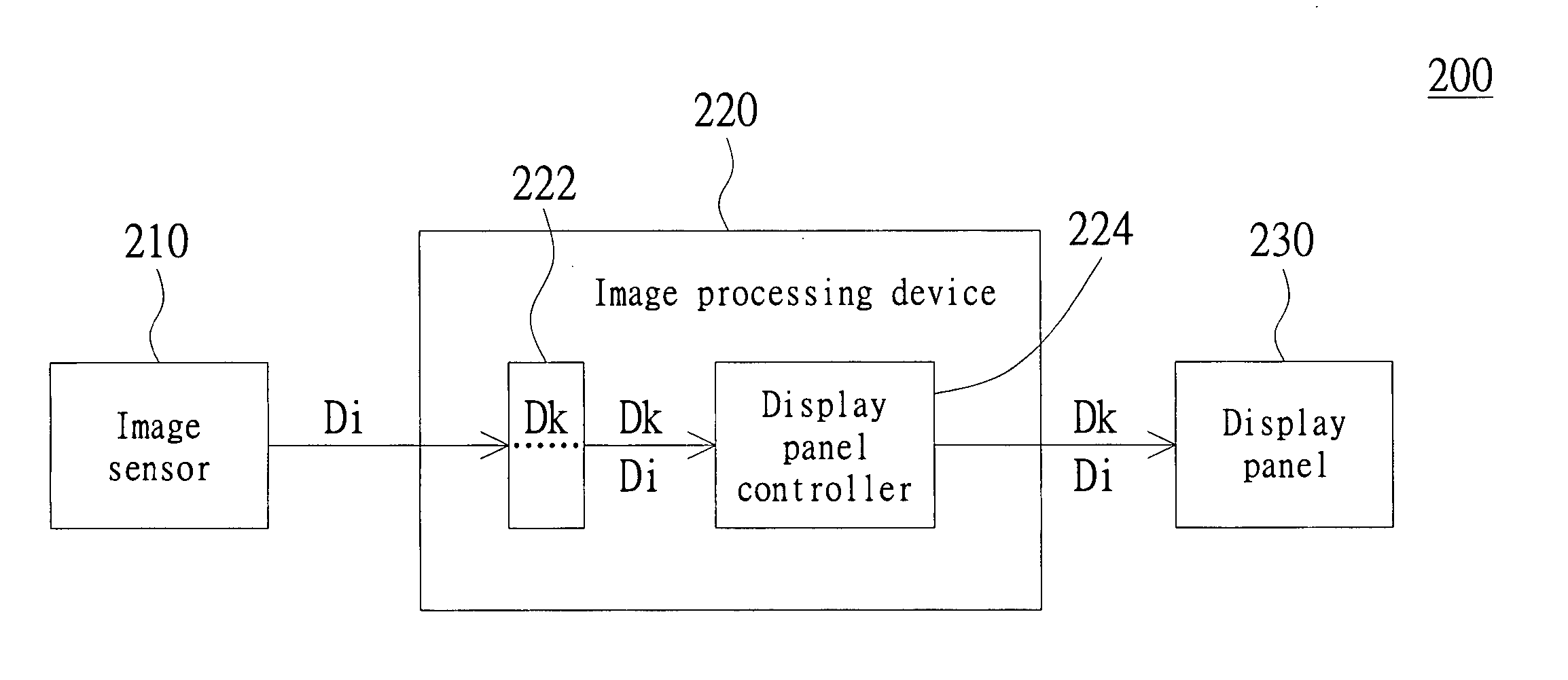
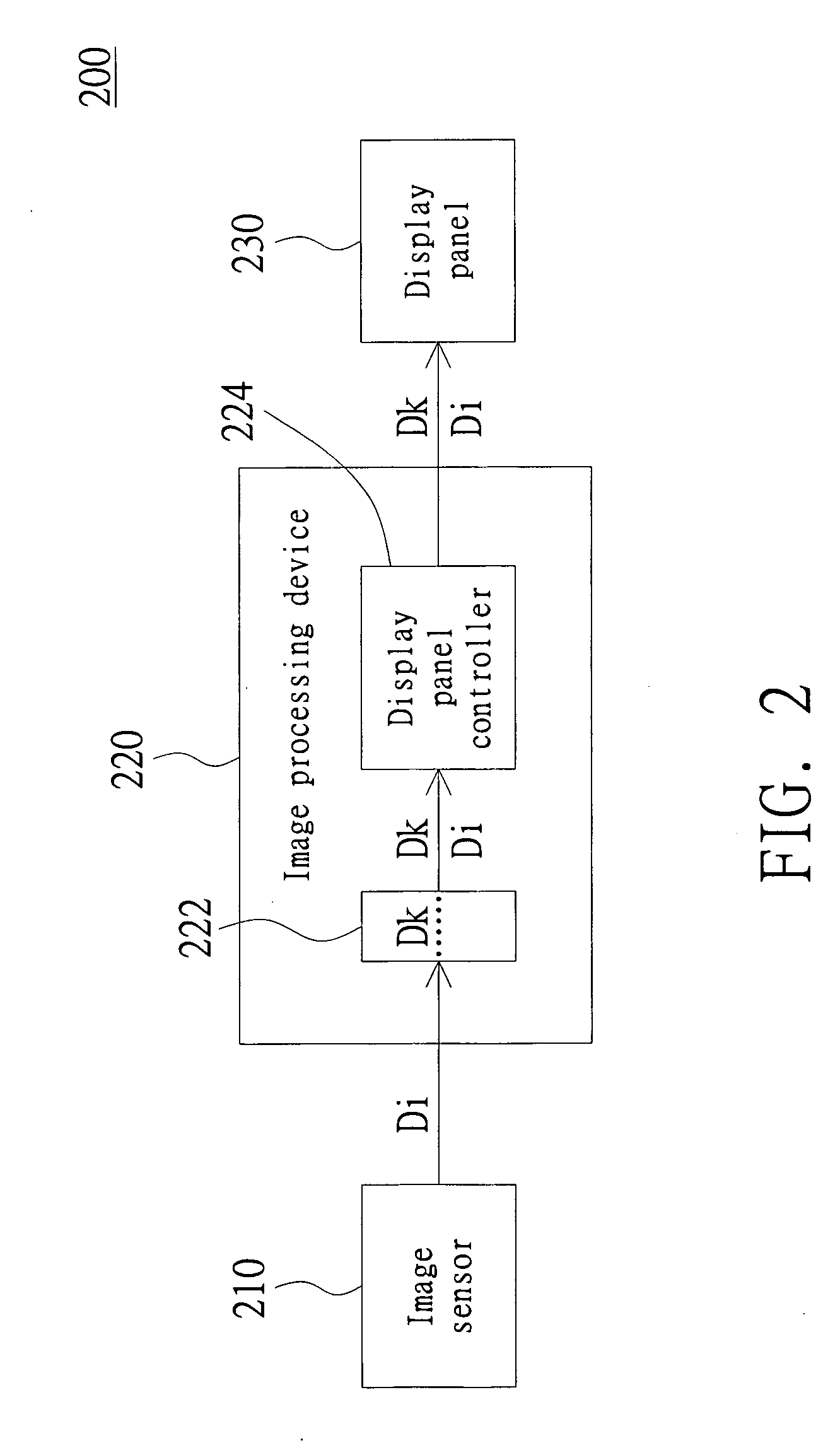
[0012] Referring to FIG. 2 is a block diagram illustrating the structure of the mobile phone according to a preferred embodiment of the invention. The mobile phone 200 includes an image sensor 210, an image processing device 220 and a display panel 230. The image processing device 220 includes memory 222 and a display panel controller 224. The image processing device 220 is used to digitize and store the image data Di captured by the image sensor 210 or process and transmit the digitized image data Dk derived from the image data Di to the display panel 230. The memory 222, for example, First In first Out (FIFO) memory, is used to store digitized image data Dk. When the image data Dk are on demand for display, the display panel controller 224 can read, process and then transmit the digitized image data Dk from the memory 222 to the display panel 230.

[0013] Unlike the conventional image processing device 120 storing the data corresponding to a frame of image at a time, the image proc...


PUM


Abstract

An image processing device includes memory and a display panel controller. The memory is used to store digitized image data derived from the image data captured by the image sensor, and the display panel controller is used to process the digitized image data stored in the memory. A portion of the image data captured by the image sensor are directly processed by the display controller and output to the display panel.

Description

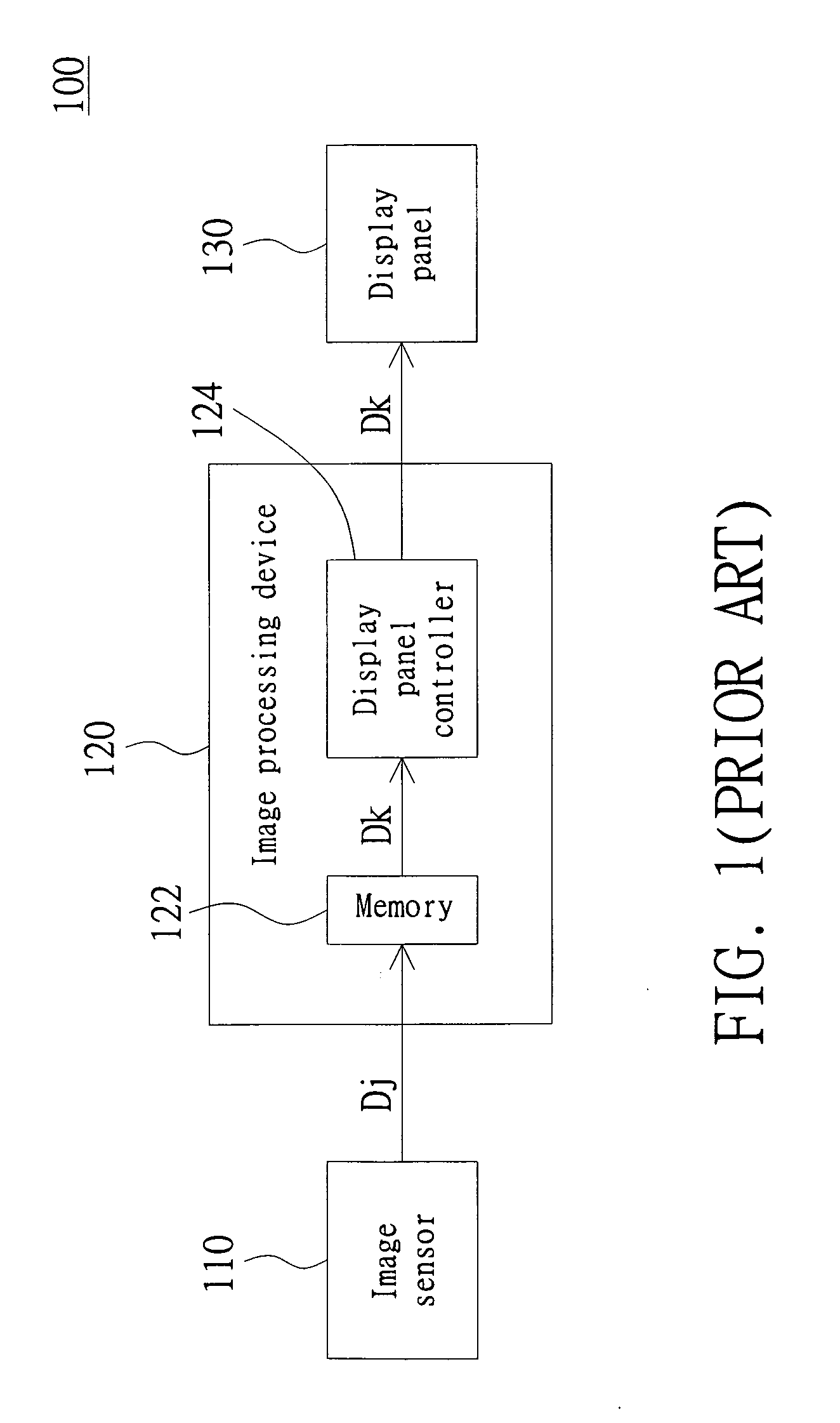
[0001] This application claims the benefit of Taiwan application Serial No. 93128381, filed Sep. 20, 2004, the subject matter of which is incorporated herein by reference. BACKGROUND OF THE INVENTION [0002] 1. Field of the Invention [0003] The invention relates to an image processing device and more particularly to an image processing device capable of saving memory space. [0004] 2. Description of the Related Art [0005]FIG. 1 is a schematic block diagram showing the structure of a conventional mobile phone. Referring to FIG. 1, the mobile phone 100 includes an image sensor 110, an image processing device 120 and a LCD display panel 130. The image processing device 120 includes memory 122 and a display panel controller 124. In general, the image data Dj captured by the image sensor 110 will be completely digitized and stored in the memory 122. When the image data Dj are to be displayed, the display panel controller 124 will read and transmit the digitized image data Dk from the memor...

Claims


Application Information

Patent Timeline
Patent Type & Authority Applications(United States)
IPC IPC(8): G09G5/00G09G5/42H04M11/00H04N5/225
CPCG09G5/42
Inventor CHENG, HAN-MINWANG, HSIU-WEN
Owner ALPHA IMAGING TECH CORP
Learn More