Plasma display panel
a technology of plasma and display panel, which is applied in the direction of gas-filled discharge tubes, electric discharge tubes, instruments, etc., can solve the problems of high y-coefficient mgo, a lot of crystal defects, and a decrease in initial emission
- Summary
- Abstract
- Description
- Claims
- Application Information
AI Technical Summary
Benefits of technology
Problems solved by technology
Method used
Image
Examples
Embodiment Construction
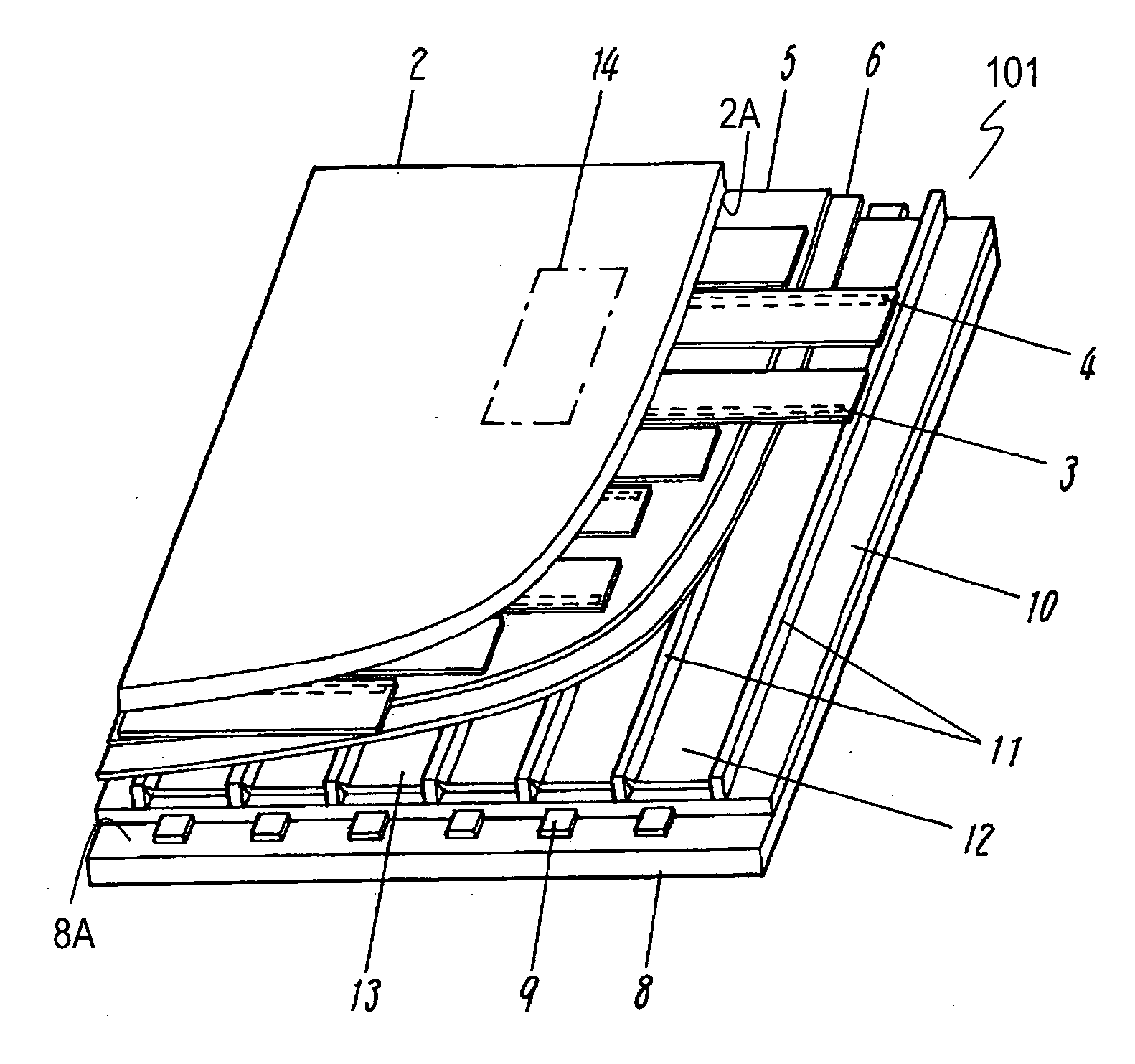
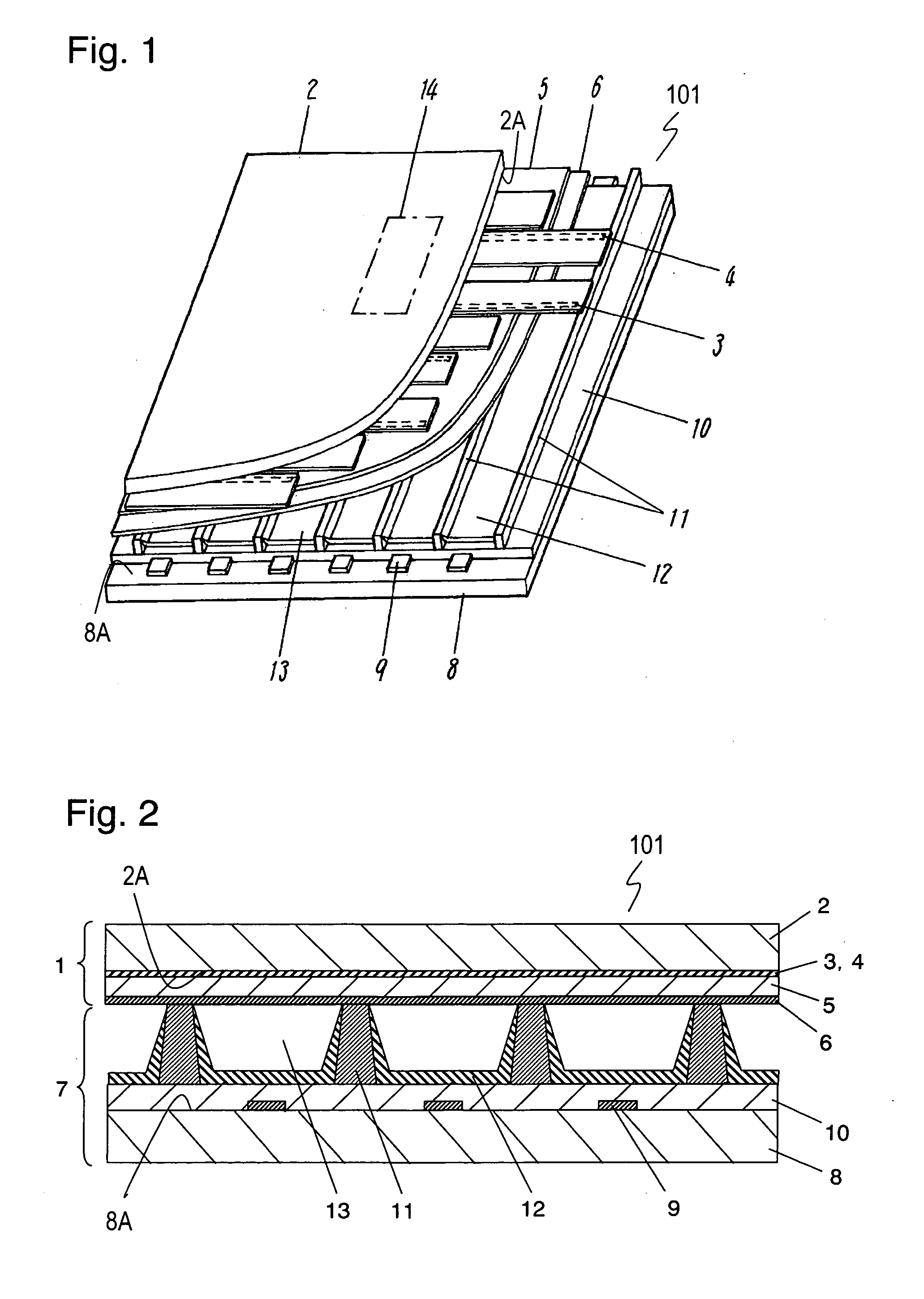
[0013]FIG. 1 is a partially-sectional, perspective view of an AC surface-discharge type plasma display panel (PDP) 101 for schematically illustrating a structure of the PDP. FIG. 2 is a sectional view of PDP 101.
[0014] In front panel 1, a pair of stripe scan electrode 3 and stripe sustain electrode 4 forms a display electrode. Plural pairs of scan electrode 3 and sustain electrode 4, i.e. plural of display electrodes, are provided on surface 2A of front glass substrate 2. Dielectric layer 5 covers scan electrode 3 and sustain electrode 4 is formed, and protective layer 6 for covering dielectric layer 5 is formed.
[0015] In rear panel 7, stripe address electrode 9 is provided on surface 8A of rear glass substrate 8 perpendicularly to scan electrode 3 and sustain electrode 4. Electrode protective layer 10 covering address electrode 9 protects address electrode 9, and reflects visible light in a direction towards front panel 1. Barrier ribs 11 are provided on electrode protective laye...
PUM
 Abstract
Description
Claims
Application Information
 - R&D
- Intellectual Property
- Life Sciences
- Materials
- Tech Scout
- Unparalleled Data Quality
- Higher Quality Content
- 60% Fewer Hallucinations
Browse by: Latest US Patents, China's latest patents, Technical Efficacy Thesaurus, Application Domain, Technology Topic, Popular Technical Reports.
© 2025 PatSnap. All rights reserved.Legal|Privacy policy|Modern Slavery Act Transparency Statement|Sitemap|About US| Contact US: help@patsnap.com


