
Process for producing optical waveguide

a technology of optical waveguides and process steps, applied in the direction of photosensitive materials, instruments, photomechanical apparatuses, etc., can solve the problems of inability to stably form optical waveguides in terms of shape, inability to achieve cost reduction, and improve suitability

Inactive Publication Date: 2006-02-09
NITTO DENKO CORP
View PDF3 Cites 9 Cited by
  • Summary
  • Abstract
  • Description
  • Claims
  • Application Information

AI Technical Summary

Benefits of technology

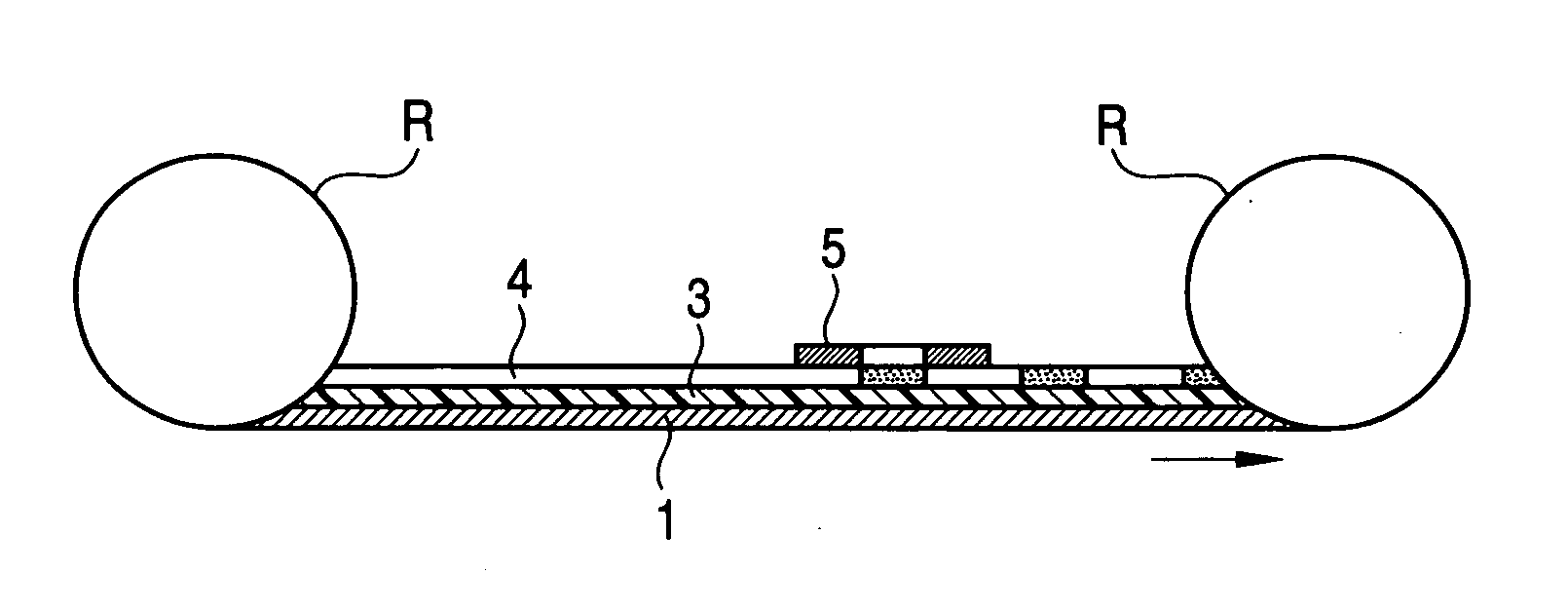
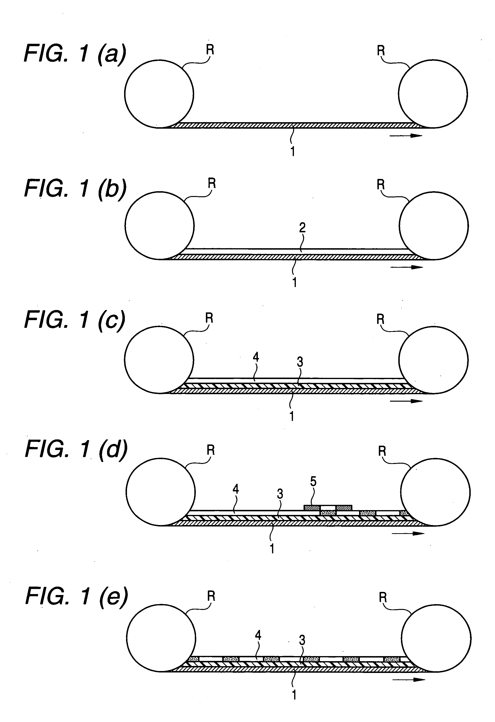
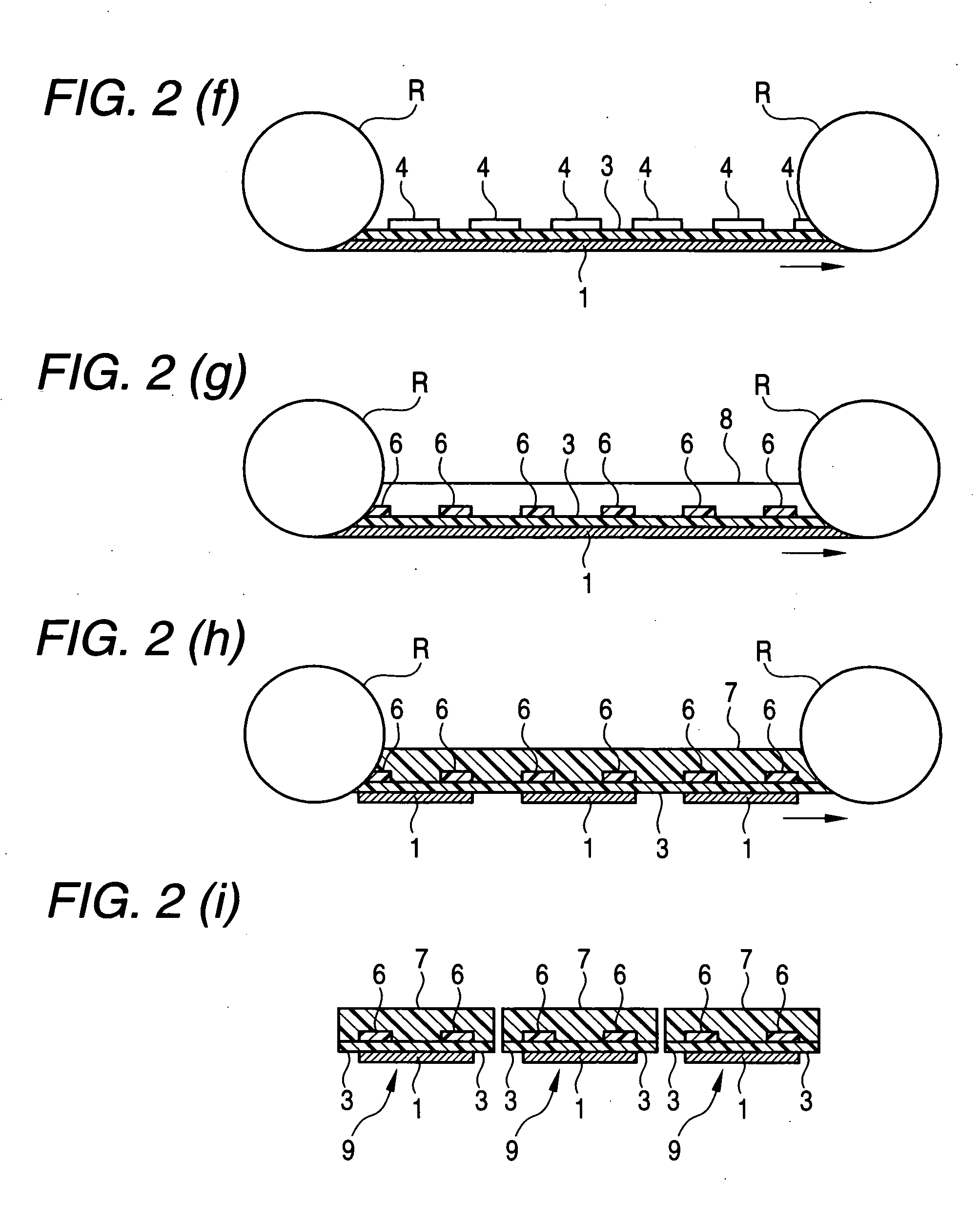
[0009] The above-described objects of the invention have been achieved by providing a process for producing an optical waveguide, comprising the steps of:
[0010] continuously applying a fluorene derivative layer onto a continuous substrate and curing the layer to thereby form a lower cladding layer;
[0011] continuously applying a photosensitive fluorene derivative layer onto the lower cladding layer;
[0012] continuously exposing the applied photosensitive fluorene derivative layer to a light through a photomask having a predetermined pattern;
[0013] continuously subjecting the exposed photosensitive fluorene derivative layer to post-exposure heating;
[0014] continuously developing the heated photosensitive fluorene derivative layer to remove the unexposed areas therein, thereby forming into the predetermined pattern;

Problems solved by technology

However, the process described in patent document 1 has limitations in improving suitability for mass production and attaining a cost reduction based on the suitability for mass production, because the optical waveguides in the process are produced on a silicon substrate by a sheet-by-sheet method (batch method).
Furthermore, the use of a liquid photosensitive resin has drawbacks that fouling of a photomask may occur in handling the liquid resin and that due to the flowability of the liquid, optical waveguides cannot be stably formed in terms of shape.

Method used


Image

  • Process for producing optical waveguide
  • Process for producing optical waveguide
  • Process for producing optical waveguide

Examples


examples

[0103] The present invention will be illustrated in greater detail with reference to the following Examples, but the invention should not be construed as being limited thereto.

Preparation of Varnishes

[0104] According to each of the formulations shown in Table 1, the ingredients were mixed and dissolved using cyclohexanone as a solvent. Thus, a fluorene derivative varnish A and a photosensitive fluorene derivative varnish B were prepared. The refractive indexes, as measured at a wavelength of 633 nm, of cured resins respectively obtained by curing these varnishes are also shown in Table 1.

TABLE 1(parts by weight)PhotosensitiveFluorenefluorenederivativederivativeVarnishvarnish Avarnish BFluorene derivative 18367Fluorene derivative 233Diluent17Photo-acid generator11Refractive index of curedresin1.5851.617(measuring wavelength, 633nm)

Fluorene derivative 1:

Bisphenoxyethanolfluorene diglycidyl ether (represented by general formula (1) wherein R1 to R6 each are a hydrogen atom or n =...


PUM

PropertyMeasurementUnit
lengthaaaaaaaaaa
lengthaaaaaaaaaa
lengthaaaaaaaaaa

Abstract

The present invention provides a process for producing an optical waveguide, comprising the steps of: continuously applying a fluorene derivative layer onto a continuous substrate and curing the layer to thereby form a lower cladding layer; continuously applying a photosensitive fluorene derivative layer onto the lower cladding layer; continuously exposing the applied photosensitive fluorene derivative layer to a light through a photomask having a predetermined pattern; continuously subjecting the exposed photosensitive fluorene derivative layer to post-exposure heating; continuously developing the heated photosensitive fluorene derivative layer to remove the unexposed areas therein, thereby forming into the predetermined pattern; curing the developed photosensitive fluorene derivative layer to thereby form a core layer having the predetermined pattern on the lower cladding layer; and continuously applying a fluorene derivative layer over the lower cladding layer so as to cover the core layer and curing the fluorene derivative layer to thereby form an upper cladding layer.

Description

FIELD OF THE INVENTION [0001] The present invention relates to a process for producing an optical waveguide. More particularly, the invention relates to a process for producing an optical waveguide for optically connecting optical devices to each other. BACKGROUND OF THE INVENTION [0002] Optical waveguides, which are used for optically connecting optical devices to each other, are being developed because optical communication systems have come to be practically used as a result of the development of optical fibers. [0003] It has been proposed to produce such an optical waveguide by a process in which a liquid photosensitive resin such as, e.g., an epoxy oligomer or acrylic oligomer is applied onto a lower cladding layer and the resultant coating is exposed to a light through a mask and then developed with a solvent to thereby form a core layer having a predetermined pattern (see, for example, patent document 1). [0004] Patent Document 1: JP 10-268152 A [0005] However, the process de...

Claims


Application Information

Patent Timeline
Patent Type & Authority Applications(United States)
IPC IPC(8): G02B6/10G03C1/725G03C1/73
CPCG02B6/138G02B1/045G02B6/02333B05D2256/00G02B2006/12176
Inventor MUNE, KAZUNORIMOCHIZUKI, AMANESHIMIZU, YUSUKENAITOU, RYUUSUKEUSUI, HIDEYUKI
Owner NITTO DENKO CORP
Learn More