Semiconductor device and method for manufacturing the same
- Summary
- Abstract
- Description
- Claims
- Application Information
AI Technical Summary
Benefits of technology
Problems solved by technology
Method used
Image

Examples
first embodiment
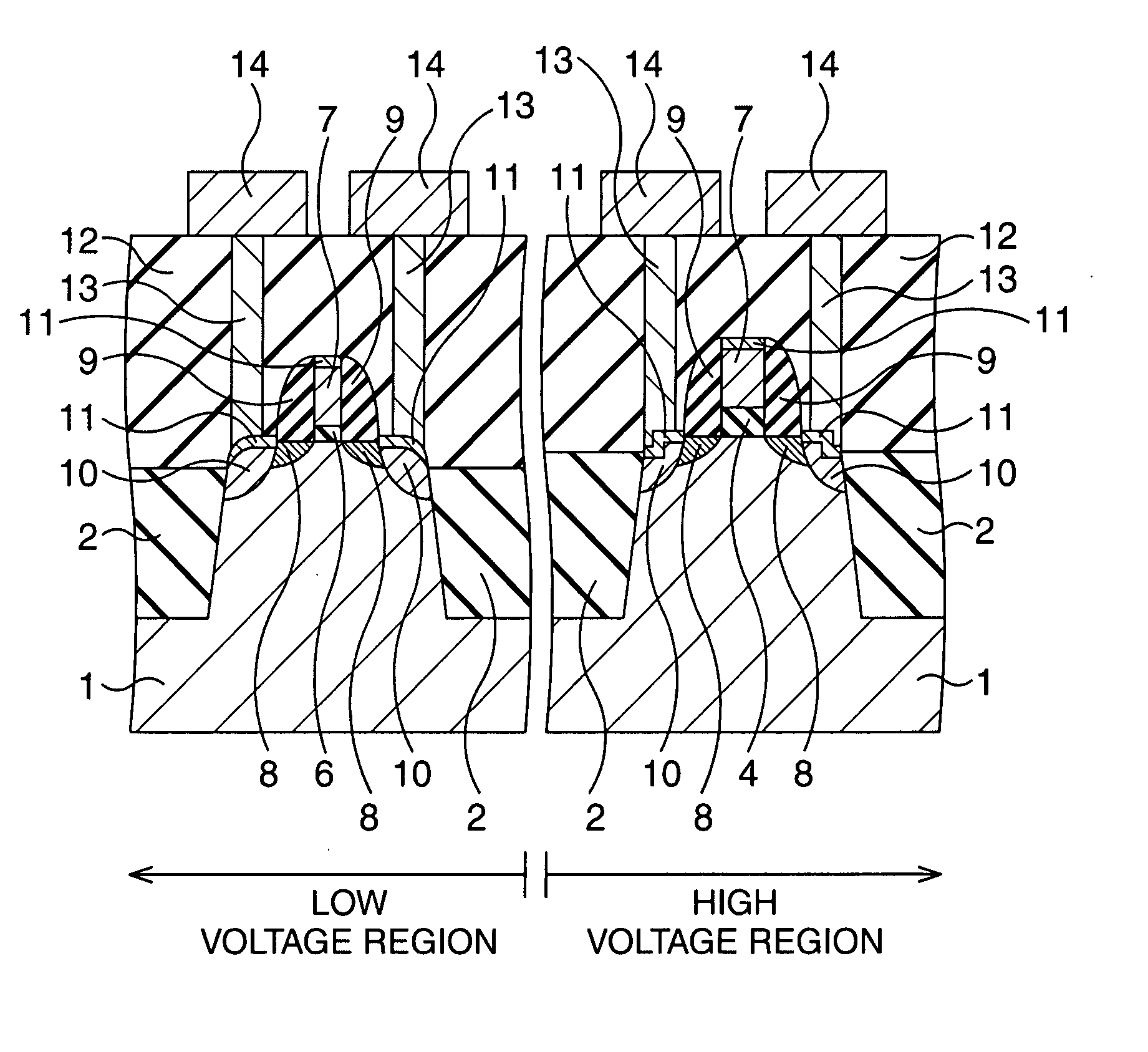
[0035] First, a first embodiment of the present invention will be described. FIG. 5A to FIG. 5J are cross-sectional views showing a method for manufacturing a semiconductor device according to the first embodiment of the present invention in the order of process steps. Besides, FIG. 6 is a plan view of the cross section shown in FIG. 5G, and the cross section taken along a I-I line in FIG. 6 is FIG. 5G. FIG. 7 is a cross-sectional view showing the cross section perpendicular to the cross section shown in FIG. 5G. FIG. 8 is a plane view of the cross section shown in FIG. 7, and the cross section taken along a II-II line in FIG. 8 is FIG. 7.
[0036] In the first embodiment, a semiconductor device including two kinds of MOS transistors different, for example, in thickness of the gate insulating film are manufactured. A region where a MOS transistor including a thin gate insulating film (a low voltage transistor) will be formed is referred to as a low voltage region, and a region where a...
second embodiment
[0049] Next, a second embodiment of the present invention will be described. FIG. 9A to FIG. 9F are cross-sectional views showing a method for manufacturing a semiconductor device according to the second embodiment of the present invention in the order of process steps. In the second embodiment, RTH is performed also on the high voltage transistor.
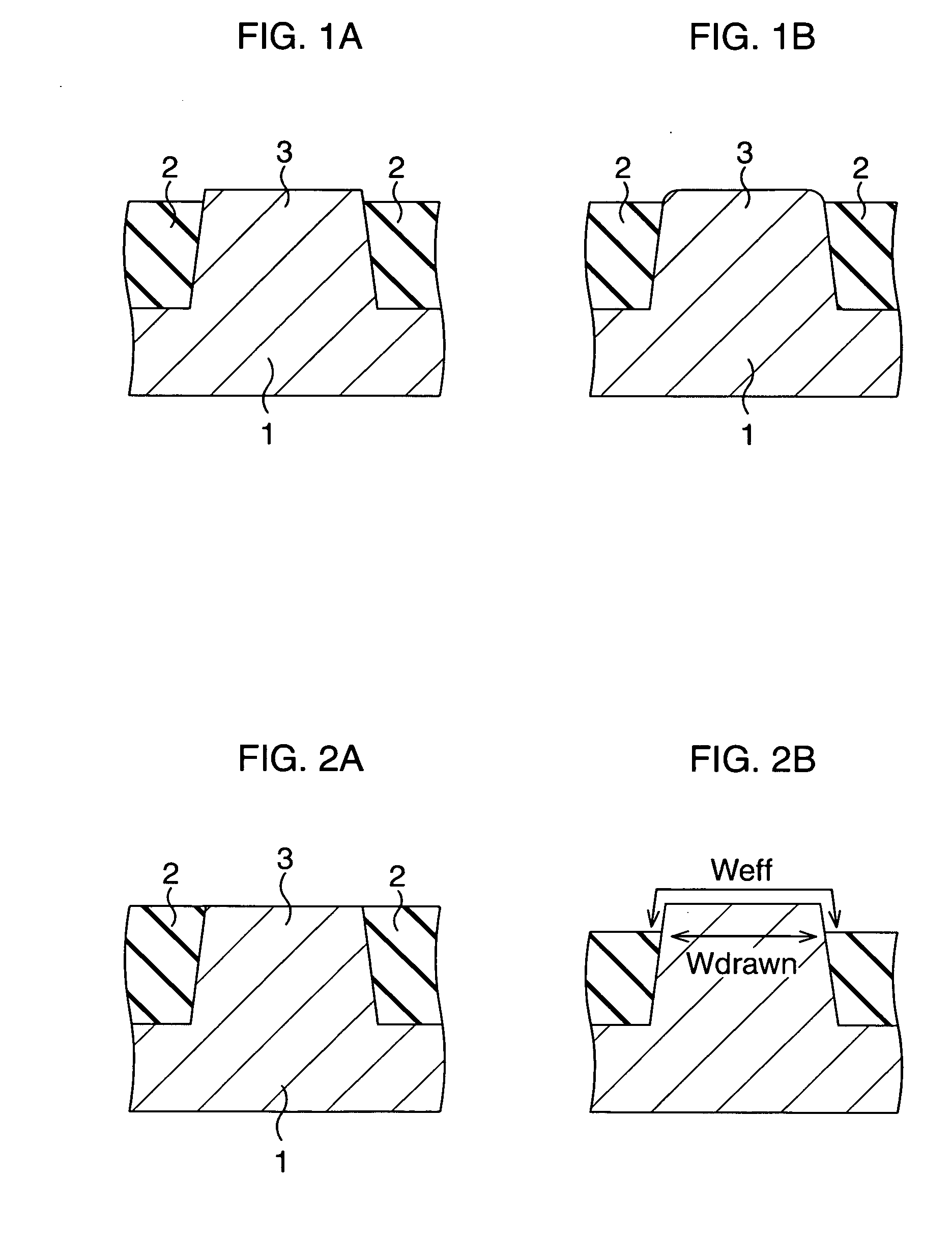
[0050] In the second embodiment, first, as shown in FIG. 9A, element isolation insulating films 2 are formed on a semiconductor substrate, for example, a Si substrate 1 to thereby define active regions 3. In this event, the surfaces of the element isolation insulating films 2 may be at a position lower than the surfaces of the active regions 3 by, for example, about 8 nm.
[0051] Next, RTH is performed on respective regions 3a within the high voltage region and the low voltage region. As a result of this, as shown in FIG. 9B, a natural oxide film is removed from the surfaces of the active regions 3 so that the flatness of the active region...
third embodiment
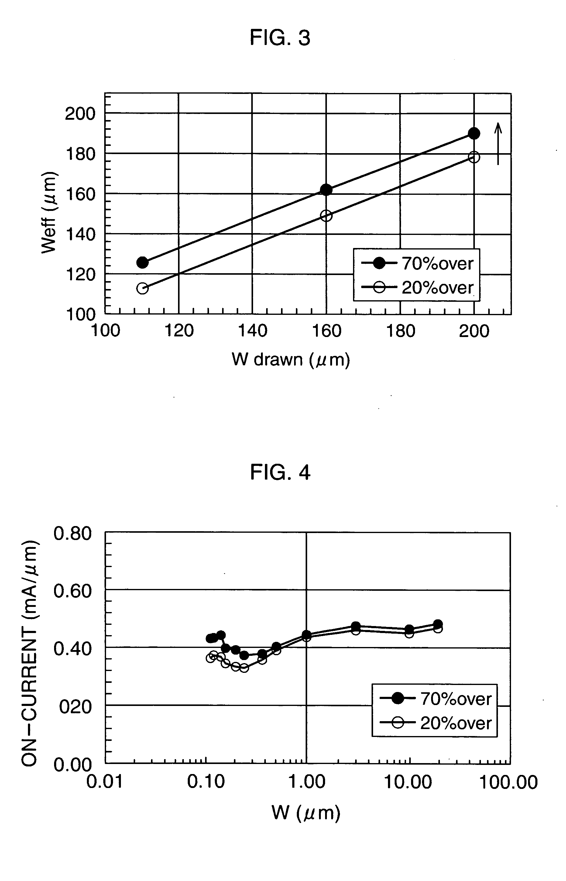
[0058] Next, a third embodiment of the present invention will be described. Manufacturing of such a plurality of kinds of semiconductors may be generally demanded that operation voltages of low voltage transistors are equal but operation voltages of high voltage transistors are different. In such a case, the thicknesses of their gate insulating films for the high voltage transistors will be different, leading to different Si-consumptions within active regions in forming the gate insulating films. For example, the Si-consumption when forming a 3 nm-gate insulating film 4a for a high voltage transistor is about 1.35 nm as shown in FIG. 10A, while the Si-consumption when forming a 7.45 nm-gate insulating film 4b under the same conditions is about 3.35 nm as shown in FIG. 10B. As a result of this, there occurs a difference of 2 nm between the active region and the element isolation insulating film after the formation of the gate oxide film. Accordingly, overetching performed on all of t...
PUM
 Abstract
Description
Claims
Application Information
 - R&D
- Intellectual Property
- Life Sciences
- Materials
- Tech Scout
- Unparalleled Data Quality
- Higher Quality Content
- 60% Fewer Hallucinations
Browse by: Latest US Patents, China's latest patents, Technical Efficacy Thesaurus, Application Domain, Technology Topic, Popular Technical Reports.
© 2025 PatSnap. All rights reserved.Legal|Privacy policy|Modern Slavery Act Transparency Statement|Sitemap|About US| Contact US: help@patsnap.com