Pattern analysis method, pattern analysis apparatus, yield calculation method and yield calculation apparatus
a pattern analysis and pattern analysis technology, applied in the direction of instrumentation, program control, cad circuit design, etc., can solve the problems of contact failure, random defect failure probability derived from random defects, and inability to accurately obtain the probability of via failur
- Summary
- Abstract
- Description
- Claims
- Application Information
AI Technical Summary
Benefits of technology
Problems solved by technology
Method used
Image

Examples
embodiment 1
Modification of Embodiment 1
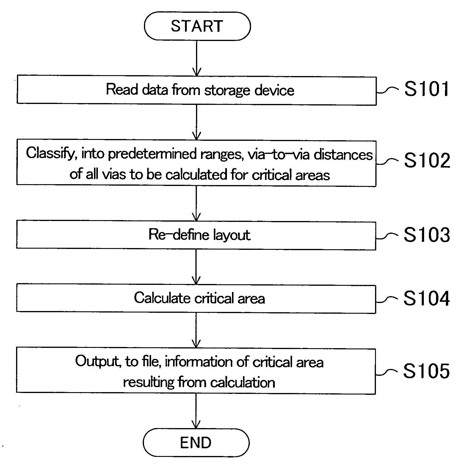
[0112] A pattern analysis method, a pattern analysis apparatus, a yield calculation method and a yield calculation apparatus according to a modification of Embodiment 1 of the invention will now be described with reference to the accompanying drawings by exemplifying pattern analysis and yield calculation of an electronic device including a plurality of vias, such as a semiconductor device.
[0113] Also in this modification, failures of vias (via connection failures) are divided into open failures and short failures, and a yield of vias derived from the open failures is calculated as in Embodiment 1. However, in this modification, the open failures of vias are further divided into soft open failures and hard open failures differently from Embodiment 1. In this case, it is necessary to divide evaluation results of a test chip into short, soft open and hard open for calculating the yield. Also, in the case where a critical area is to be calculated on the bas...
embodiment 2
[0123] A pattern analysis method and a pattern analysis apparatus according to Embodiment 2 of the invention will now be described with reference to the accompanying drawings by exemplifying pattern analysis of an electronic device including a plurality of vias, such as a semiconductor device.
[0124] Differently from Embodiment 1, as a characteristic of this embodiment, a hard open critical area and a soft open critical area described in the modification of Embodiment 1 are calculated by using the geometry method (see, for example, Non-patent document 6) or the Monte Carlo method (see, for example, Non-patent document 7) conventionally widely used.
[0125]FIGS. 10A through 10C are diagrams for explaining a critical area calculation method of this embodiment performed by using, for example, the Monte Carlo method.
[0126] First, in the same manner as in the modification of Embodiment 1, each via 120 is divided into a hard open critical area calculation via region 120A whose center acco...
embodiment 3
[0135] A yield calculation method and a yield calculation apparatus according to Embodiment 3 of the invention will now be described with reference to the accompanying drawings by exemplifying yield calculation of an electronic device including a plurality of vias such as a semiconductor device.
[0136]FIG. 11A shows the plan structure of a test chip used in this embodiment. As shown in FIG. 11A, a via chain composed of a lower interconnect 101, an upper interconnect 102 and vias 103 connecting them to each other is provided on the test chip.
[0137] Now, a method for obtaining the yield of vias by actually using the test chip of FIG. 11A and a method for obtaining a defect density of the vias on the basis of the obtained yield will be described in detail.
[0138] First, critical areas Ecalower, Ecaupper and Ecavia of the upper interconnect, the lower interconnect and the via are obtained by using the layout of the via chain. At this point, graphic data processing by a conventional met...
PUM
 Abstract
Description
Claims
Application Information
 - R&D
- Intellectual Property
- Life Sciences
- Materials
- Tech Scout
- Unparalleled Data Quality
- Higher Quality Content
- 60% Fewer Hallucinations
Browse by: Latest US Patents, China's latest patents, Technical Efficacy Thesaurus, Application Domain, Technology Topic, Popular Technical Reports.
© 2025 PatSnap. All rights reserved.Legal|Privacy policy|Modern Slavery Act Transparency Statement|Sitemap|About US| Contact US: help@patsnap.com