Coms buffer having higher and lower voltage operation

a buffer and lower voltage technology, applied in the field of integrated circuits, can solve the problems of shortening the battery life, requiring a larger power source, and being vulnerable to external voltage and curren

Inactive Publication Date: 2005-12-08
AGERE SYST INC
View PDF2 Cites 7 Cited by
  • Summary
  • Abstract
  • Description
  • Claims
  • Application Information

AI Technical Summary

Problems solved by technology

While direct electrical connection with internal components of an IC is possible, it would leave the IC vulnerable to external voltages and currents, which may exceed the ability of the internal circuit.
Though a necessary evil, buffers can utilize excess power in a given application, shortening battery life, requiring larger power sources, etc.
Excess use of power can be particularly troublesome where a buffer is operable with multiple voltage levels, e.g., 3.3v, 2.5v, etc.
Known voltage translator circuits that allow the normally “lower” voltage signals to be translated up in voltage to the “higher” voltage values does not work very well if the “higher” voltage is equal to the “lower” voltage value.
Moreover, conventional voltage translator circuits produce very long delays, and more importantly a very large skew, in the signal path when the “higher” voltage level is lowered down to the “lower” voltage level.
In fact, the gate-to-source voltage VGS would be equal to 3.3V−1.2V=2.1V, which would produce a waste of a large amount of power.
Moreover, and importantly, there is an inherent skew to the output of the translator-up circuit X4, X5.
This produces a skew on the circuits output signal, caused by this delay between transition directions.

Method used


Image

  • Coms buffer having higher and lower voltage operation
  • Coms buffer having higher and lower voltage operation
  • Coms buffer having higher and lower voltage operation

Examples


Embodiment Construction

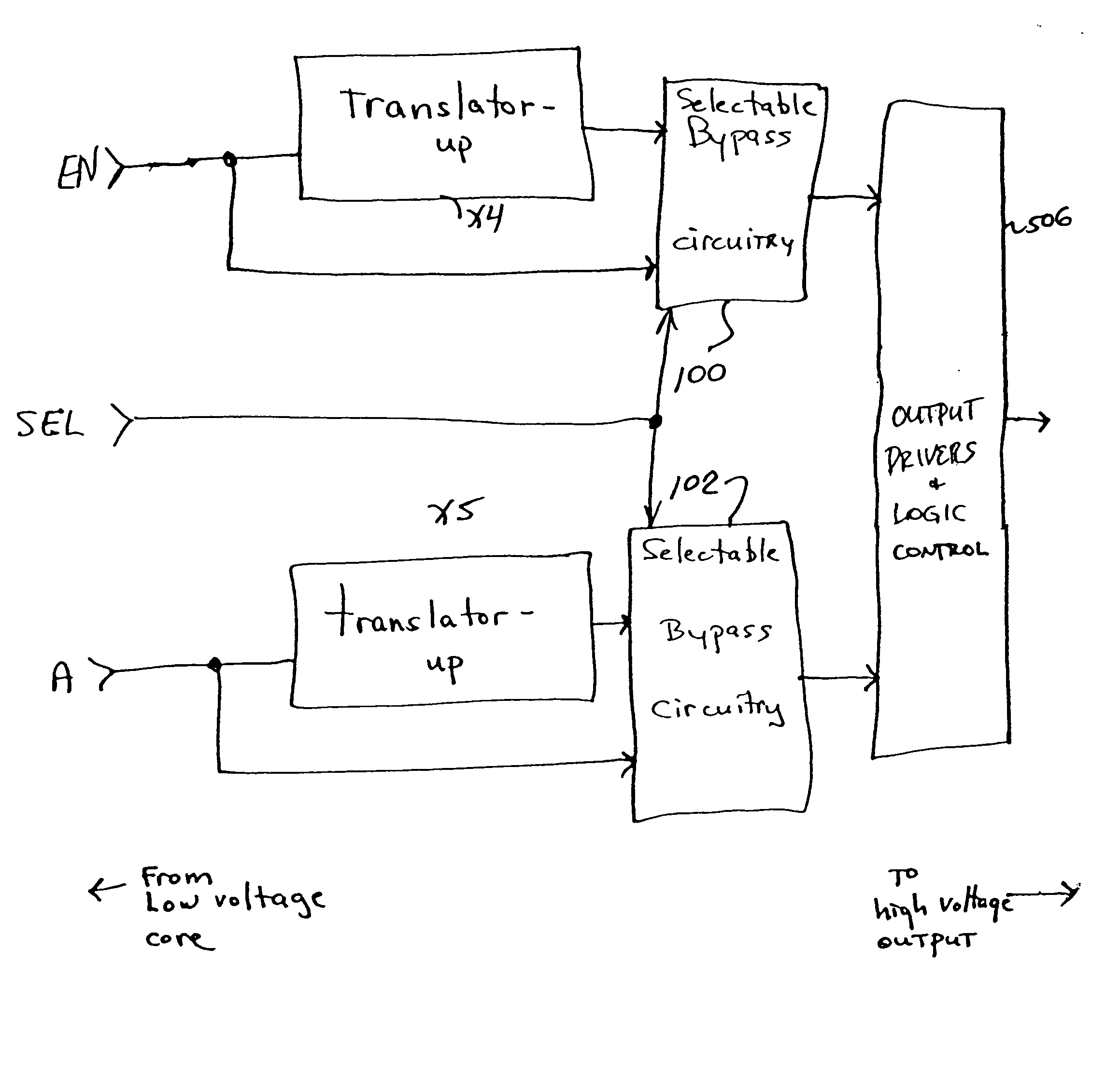
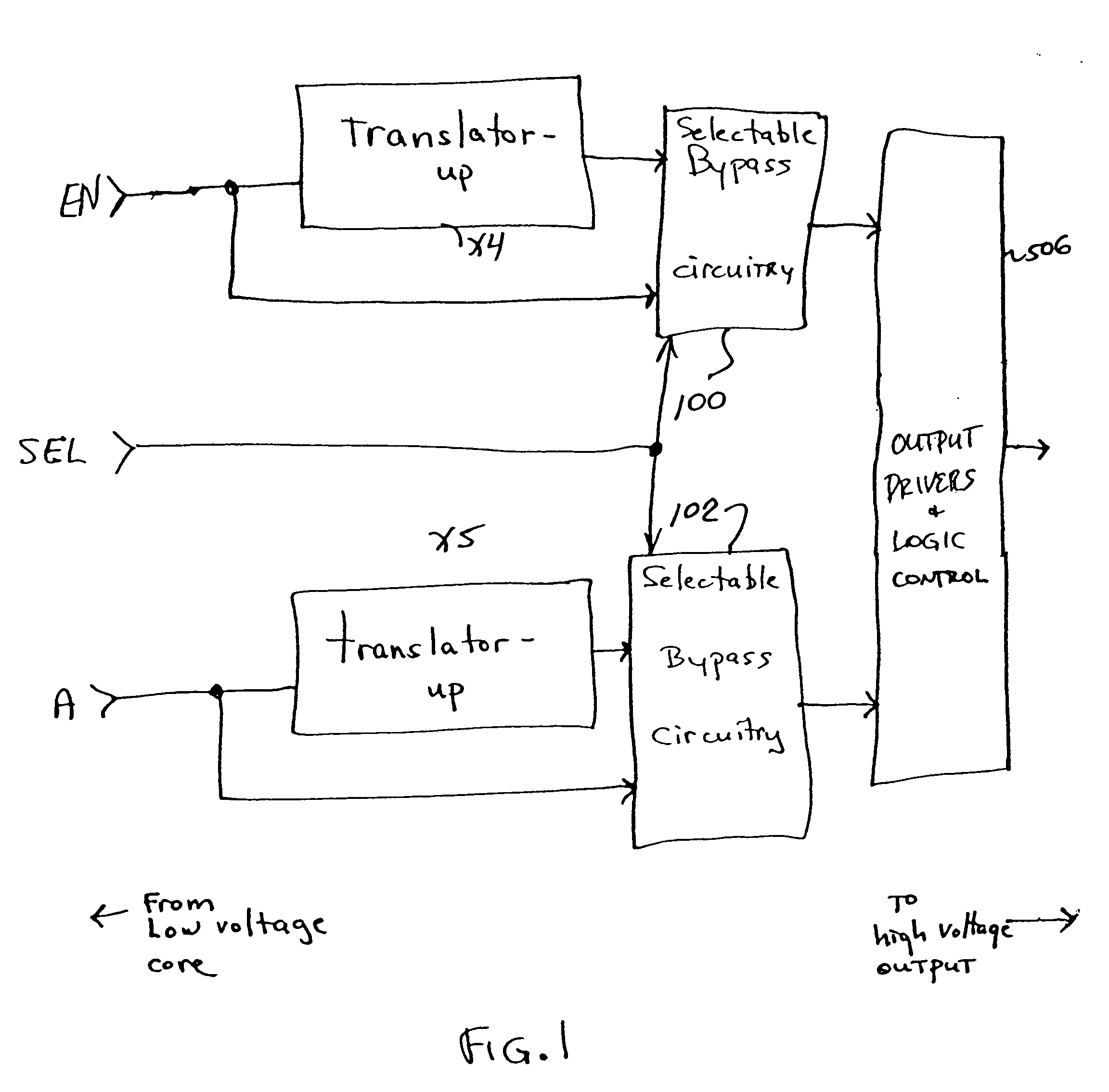
[0037] The present invention provides a buffer design for an integrated circuit that not only recognizes, but improves upon the skew problem as described above that is particularly problematic in cases where the output buffer supply voltage is particularly close or the same as the voltage of the signals coming from the core of an IC.

[0038] In accordance with the principles of the present invention, translator-up circuits associated with output buffers are implemented in parallel with respective selectable bypass circuits, allowing the translator-up circuit to be inserted into or removed from a signal path based on the voltage level of a signal received from the inner core and the voltage level required by the output buffer. When the voltage level of the “higher” voltage side is equal to the voltage level of the “lower” voltage side, the translator-up circuits are bypassed through selection by a selectable bypass circuit, such as a multiplexer. Thus, a selectable bypass circuit is i...


PUM


Abstract

A buffer design for an integrated circuit that not only recognizes, but improves upon the skew problem as described above that is particularly problematic in cases where the output buffer supply voltage is particularly close or the same as the voltage of the signals coming from the core of an IC. Translator-up circuits associated with output buffers are implemented in parallel with respective selective bypass circuits, allowing the translator-up circuit to be inserted into or removed from a signal path based on the voltage level of a signal received from the inner core and the voltage level required by the output buffer. When the voltage level of the “higher” voltage side is equal to the “lower” voltage signal level, the translator-up circuits are bypassed through selection by a selective bypass circuit. Thus, a selective bypass circuit is implemented together with a translator-up circuit to eliminate large signal skew, and to generally speed up circuit performance.

Description

BACKGROUND OF THE INVENTION [0001] 1. Field of the Invention [0002] This invention relates to integrated circuits. More particularly, it relates to the design of input and output buffers in an integrated circuit capable of efficient operation at multiple voltage levels. [0003] 2. Background of Related Art [0004] Integrated circuits are an important part of life as we know it today. They are the basis for most all electronic devices, from telephones and answering machines to the most sophisticated computers. An important part of an integrated circuit (IC) is its ability to accept information in, and / or to pass information out. Thus, an IC must interface with the outside world. [0005] While direct electrical connection with internal components of an IC is possible, it would leave the IC vulnerable to external voltages and currents, which may exceed the ability of the internal circuit. To provide both protection of internal components from external signals, as well as to provide amplif...

Claims


Application Information

Patent Timeline
Patent Type & Authority Applications(United States)
IPC IPC(8): H03K3/00H03K17/0412H03K17/06H03K19/0175H03K19/0185
CPCH03K17/04123H03K19/018585H03K19/018521H03K17/063
Inventor BHATTACHARYA, DIPANKARDOBRIYAL, BRIJENDRAMORRIS, BERNARD L.
Owner AGERE SYST INC
Why Eureka
Try Eureka