Hermetic pacakging and method of manufacture and use therefore
a technology of hermetic pacakging and manufacturing method, which is applied in the direction of semiconductor/solid-state device details, electrical apparatus, semiconductor devices, etc., can solve the problem of only suitable small-scale devices
- Summary
- Abstract
- Description
- Claims
- Application Information
AI Technical Summary
Benefits of technology
Problems solved by technology
Method used
Image
Examples
Embodiment Construction
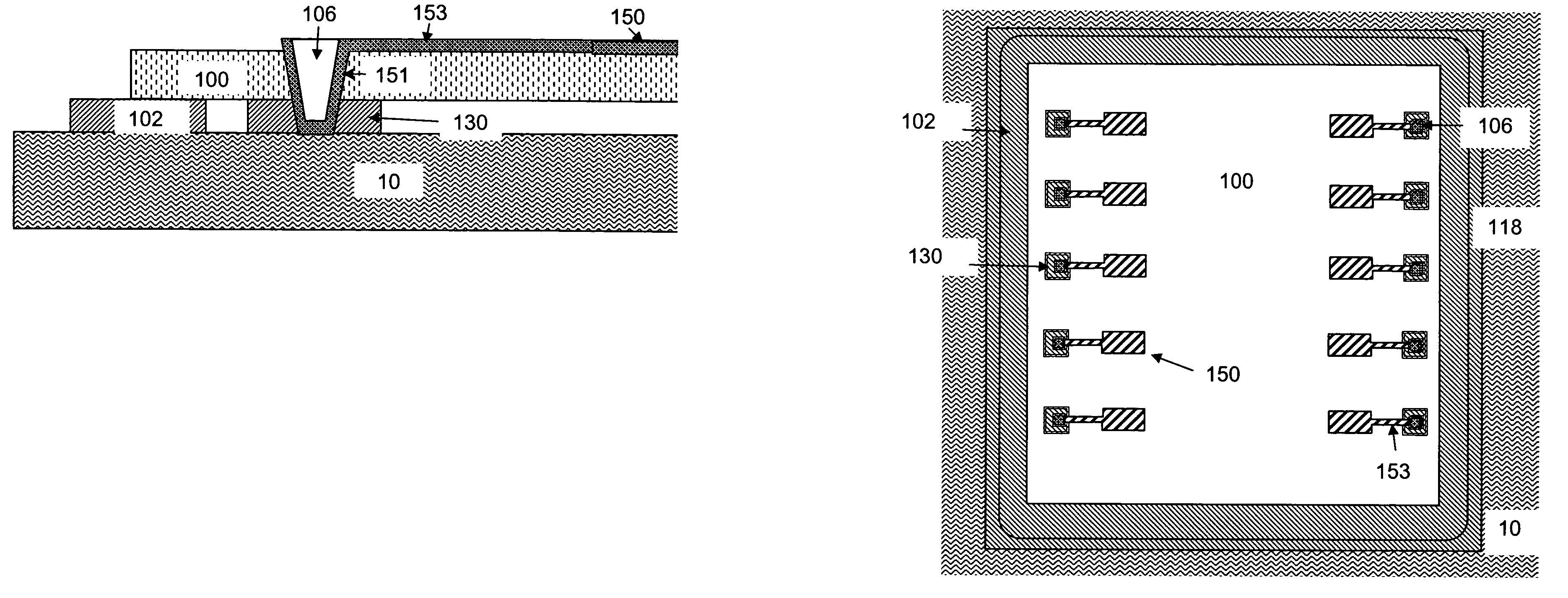
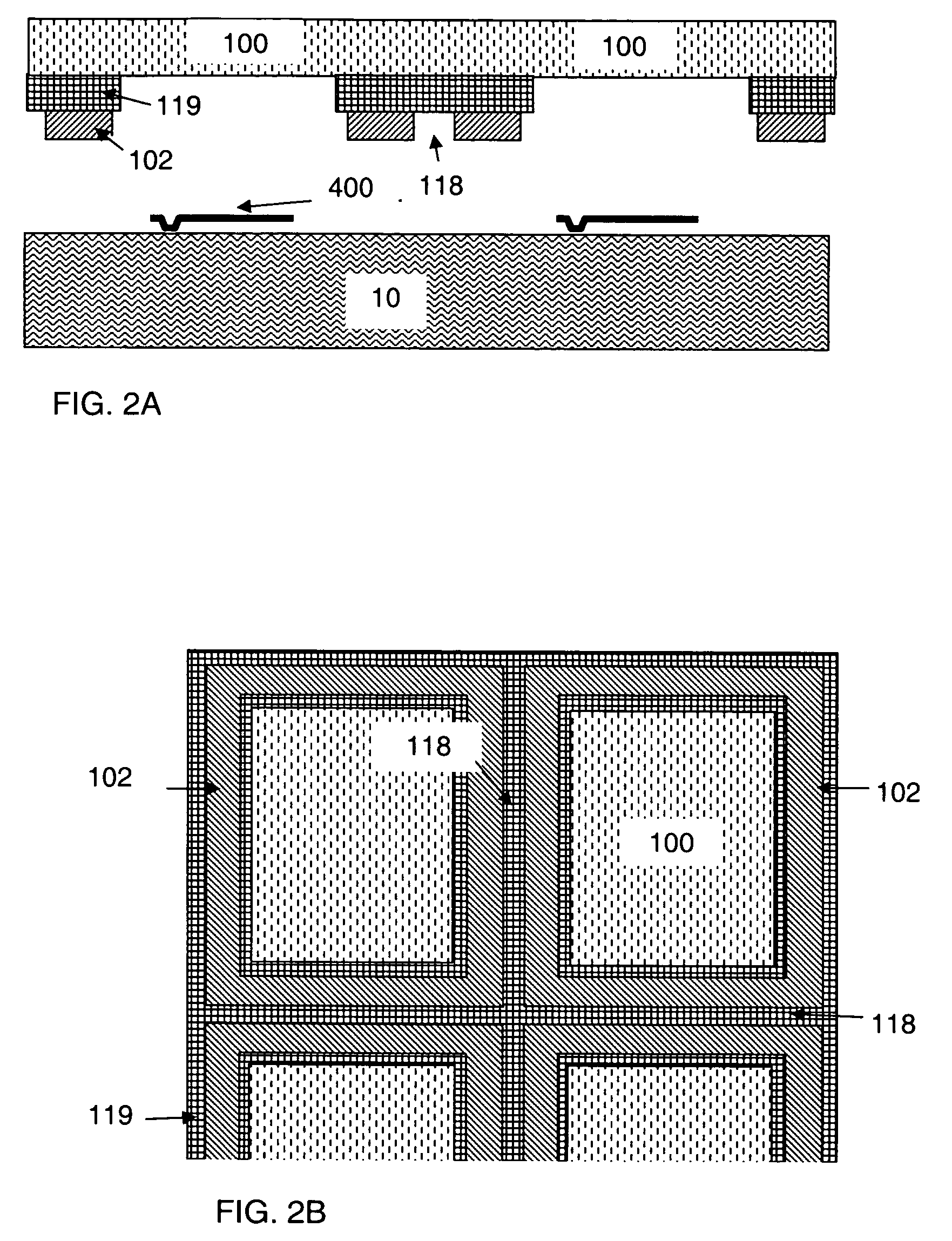
[0010] A method and system for cavity packaging MEMS devices, such as the DLP™ (digital light processor) on wafer scale in hermetic or vacuum seal is described herein. The processes of the wafer-level packaging begin during or after the final phase of the MEMS device fabrication process, and before the wafer are diced into separate chips. Referring now to FIGS. 1 to 9, there is a depicted cross-sectional view showing a particular portion of a microstructure during specific phases of the packaging process for the exemplary MEMS device. The dimensions are not shown to scale.
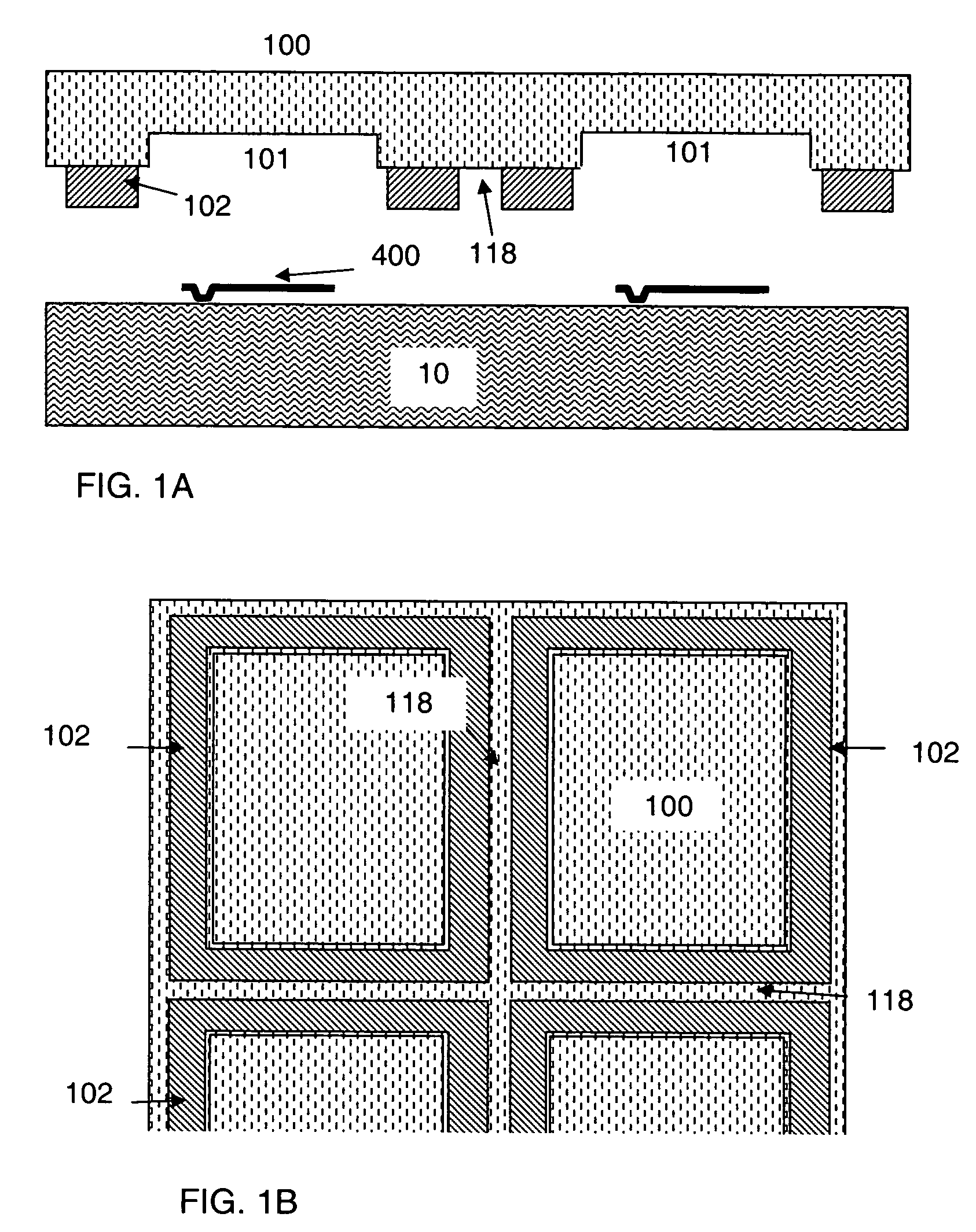
[0011]FIG. 1A depicts cross-sectional view of a microelectronics substrate 10, which comprises micromechanical structures 400, and a cap wafer 100. A plurality of adhesive rings 102, with gap 118 between them, are formed on the cap wafer 100, as shown in plain view of FIG. 1B. Alternatively the adhesive rings may be formed on the substrate wafer 10. The cap wafer 100 may have cavities 101 etched thereon and is pre...
PUM
 Abstract
Description
Claims
Application Information
 - R&D Engineer
- R&D Manager
- IP Professional
- Industry Leading Data Capabilities
- Powerful AI technology
- Patent DNA Extraction
Browse by: Latest US Patents, China's latest patents, Technical Efficacy Thesaurus, Application Domain, Technology Topic, Popular Technical Reports.
© 2024 PatSnap. All rights reserved.Legal|Privacy policy|Modern Slavery Act Transparency Statement|Sitemap|About US| Contact US: help@patsnap.com


