
Adaptable demodulator

Active Publication Date: 2005-10-27
STMICROELECTRONICS SRL
View PDF9 Cites 0 Cited by
  • Summary
  • Abstract
  • Description
  • Claims
  • Application Information

AI Technical Summary

Benefits of technology

[0017] The present invention aims at optimizing the demodulation of RF signals and in particular at increasing the possible transmission flow rates for a given clock frequency.
[0018] The present invention also aims at providing a solution which overcomes possible disturbance problems in the signal originating from an analog demodulator.

Problems solved by technology

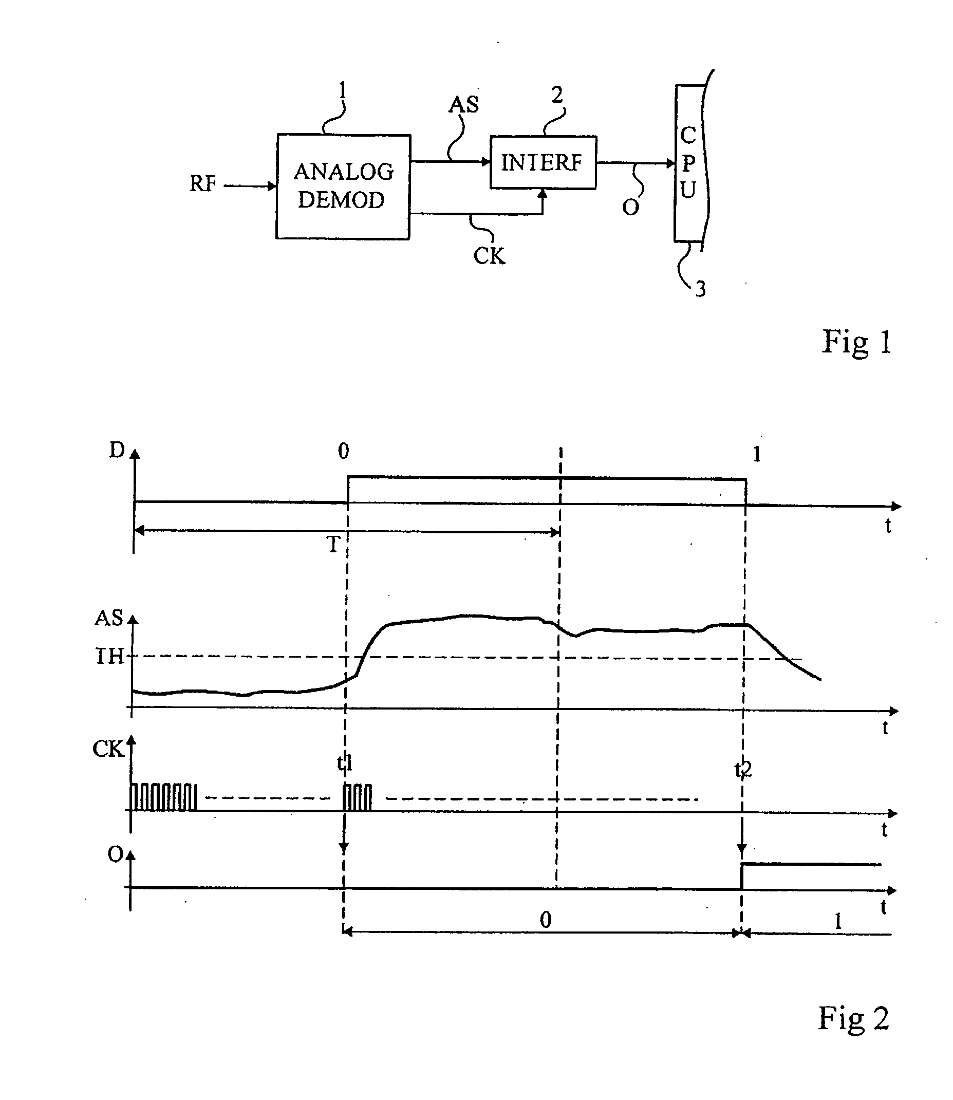
A first disadvantage of a conventional demodulation system such as illustrated in FIGS. 1 and 2 is that, if signal AS is strongly disturbed, time t1 or t2 when the signal level is taken into account risks providing an erroneous result.
Another disadvantage is that it is not possible to bring the different times of analysis of signal AS closer to one another, since this would lead to speeds incompatible with the working speed of the CPU having its clock frequency corresponding at most to the frequency of clock CK.
For example, in an application where images are desired to be transmitted (photographs, biometric prints), a flow rate of 106 kilobits per second results in transmission times of several seconds, incompatible with the desired analysis speeds.

Method used


Image

  • Adaptable demodulator
  • Adaptable demodulator
  • Adaptable demodulator

Examples


first embodiment

[0042] not shown, the analog signal originating from an analog demodulator is directly sampled at times in the symbol which correspond to the times providing the selected samples. This amounts to generating a sampling signal based on a frequency of period smaller than the duration of a symbol, but with a number of edges smaller than that of this frequency.

second embodiment

[0043] the sampling signal based on the sampling frequency directly is this frequency. The analog signal coming from the analog demodulator is then sampled at a frequency corresponding, preferably, to the maximum available frequency. The state 0 or 1 of the symbol is then deduced from several selected samples thereof.

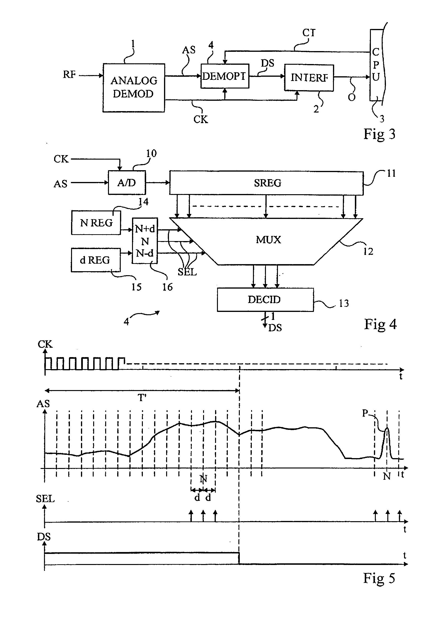
[0044]FIG. 3 very schematically shows, in the form of blocks, this second embodiment of a demodulator according to the present invention.

[0045] As previously, a radio frequency signal RF is received by an analog demodulator 2 (ANALOG DEMOD) in charge of extracting an analog signal AS as well as a clock signal CK at the frequency of the carrier which here forms the sampling signal. Signal CK is transmitted to an interface circuit 2 which provides digital signals O to a CPU 3 as in the conventional circuit of FIG. 1.

[0046] According to this embodiment of the present invention, a demodulation optimization circuit 4 (DEMOPT) is interposed between the output of analog dem...


PUM


Abstract

A method and a circuit for detecting a binary state supported by an analog symbol, comprising sampling the symbol with a sampling signal based on a frequency having a period shorter than the duration of a symbol, selecting a number of significant samples smaller than the number of samples which would be obtained with a sampling of the symbol at said frequency, and deciding of the symbol state based on the selected samples.

Description

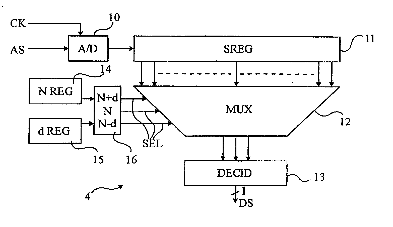
BACKGROUND OF THE INVENTION [0001] 1. Field of the Invention [0002] The present invention relates to the field of demodulators and more specifically to radio frequency signal demodulators, the results of which must be exploited by a digital processing unit. [0003] 2. Discussion of the Related Art [0004] An example of application of the present invention relates to electromagnetic transponder systems in which a transponder communicates with a contactless read-write terminal. [0005]FIG. 1 very schematically shows, in the form of blocks, the receive demodulation portion of radio frequency signals by an electromagnetic transponder. [0006] After having been received by an antenna and setup by a coupler (not shown), radio frequency signals RF are processed by an analog demodulator 1 (ANALOG DEMOD) having the function of providing a demodulated analog signal AS as well as a sampling clock CK. The sampling clock is generally taken from the transmit carrier. Signals AS and CK are sent onto a...

Claims


Application Information

Patent Timeline
IPC IPC(8): H03M1/12H04L27/06H04B1/59H04L25/06H04L25/49
CPCH04L27/06H04L25/069
Inventor GUILLOUX, YVELINEPALMADE, ROMAINROMAIN, FABRICEWUIDART, SYLVIE
Owner STMICROELECTRONICS SRL
Learn More