
Semiconductor memory device

a semiconductor and memory device technology, applied in the direction of semiconductor devices, electrical devices, transistors, etc., can solve the problems of low on/off characteristics, complicated circuits, complex devices, etc., and achieve excellent on/off characteristics and simple structur

Inactive Publication Date: 2005-10-20
KK TOSHIBA
View PDF0 Cites 2 Cited by
  • Summary
  • Abstract
  • Description
  • Claims
  • Application Information

AI Technical Summary

Benefits of technology

[0015] According to the invention, it is possible to provide a semiconductor memory device in which great restrictions are not imposed on the circuit design, fixed information and semi-fixed information can be stored in the same element, and excellent ON / OFF characteristics are attained by a simple structure.

Problems solved by technology

As a result, there arise problems in that a nonvolatile semiconductor memory device occupies a larger area, and that such a device has a complicated configuration.
However, the reversion of source and drain means that a further restriction must be imposed on the circuit design, and often causes the circuit to be complicated.
However, the proposed storage element has a problem in that charges in the charge storage layers on the source and drain sides mutually affect each other and hence has low ON / OFF characteristics.
However, this method requires means for controlling the timing of the voltage application, and hence has a problem in that the structure of a storage element is complicated and enlarged.

Method used


Image

  • Semiconductor memory device
  • Semiconductor memory device
  • Semiconductor memory device

Examples


first embodiment

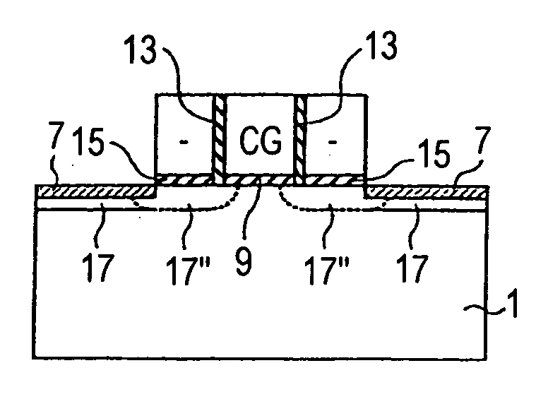
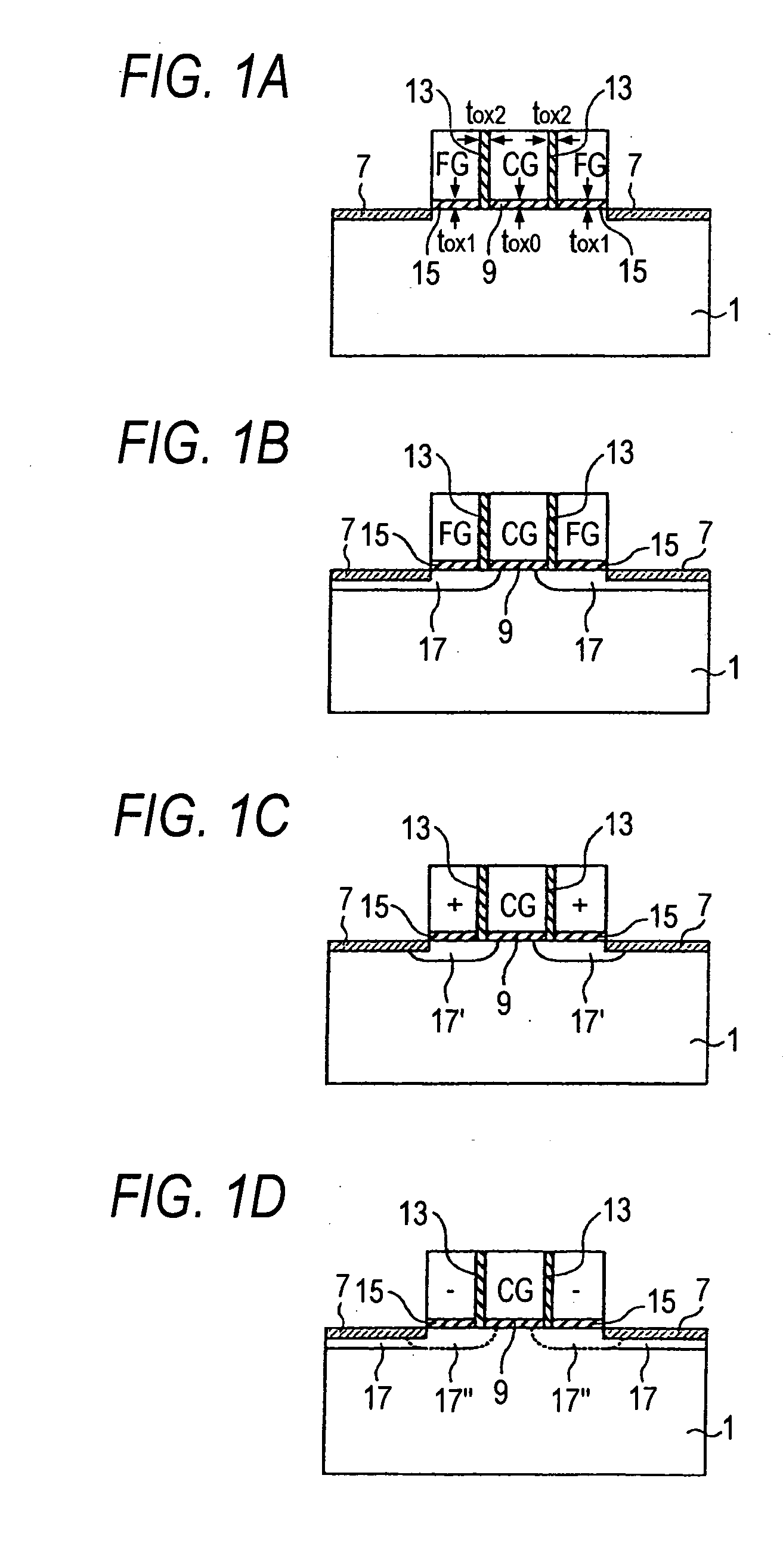
[0040] A storage element in a first embodiment will be described with reference to FIGS. 1A to 1D. A storage element is a minimum unit which independently performs a specific function in a storage device, and a storage device is a device which is formed by integrating such storage elements.

[0041]FIGS. 1A to 1D are sectional diagrams illustrating the storage element in the first embodiment, taken in the gate length direction. For the sake of convenience, a state where the amount of ON-current of the storage element is small is set as 1-state, and that where the amount of ON-current is large is set as 0-state. A case where a charge storage layer is formed by a floating gate made of a conductor which is surrounded by an insulating layer will be described.

[0042] First, a storage element in which only fixed information at factory shipment is stored will be described. FIG. 1A shows the storage element in which the fixed information is in 1-state (hereinafter, referred to as fixed inform...

second embodiment

[0110] A storage element in a second embodiment will be described with reference to FIGS. 19A to 19D. For the sake of simplicity, only portions which are different from those of the first embodiment will be described.

[0111]FIGS. 19A to 19D are sectional diagrams illustrating the storage element in the second embodiment, taken in the gate length direction. FIG. 19A shows the storage element of fixed information (1), FIG. 19B shows the storage element of fixed information (0), FIG. 19C shows the storage element of fixed information (1) and semi-fixed information (0), and FIG. 19D shows the storage element of fixed information (0) and semi-fixed information (1).

[0112] As shown in FIGS. 19A to 19D, in the storage element in the second embodiment, the semiconductor substrate 1 comprises an embedded insulating layer 25.

[0113] In the second embodiment, the region of the semiconductor substrate 1 which is directly under the pseudo impurity diffusion layers 17′ and the depleted impurity d...

third embodiment

[0122] A storage element in a third embodiment will be described with reference to FIGS. 22A to 22D. For the sake of simplicity, only portions which are different from those of the first embodiment will be described.

[0123]FIGS. 22A to 22D are sectional diagrams illustrating the storage element in the third embodiment, taken in the gate length direction. FIG. 22A shows the storage element of fixed information (1), FIG. 22B shows the storage element of fixed information (0), FIG. 22C shows the storage element of fixed information (1) and semi-fixed information (0), and FIG. 22D shows the storage element of fixed information (0) and semi-fixed information (1).

[0124] As shown in FIGS. 22A to 22D, the storage element in the third embodiment has a so-called double-gate structure. The gate insulating film 9 is configured by a first gate insulating film 9a on the semiconductor substrate 1, and a second gate insulating film 9b under the semiconductor substrate 1. The gate electrode (CG) ha...


PUM


Abstract

A semiconductor memory device includes a semiconductor substrate, a gate insulating film on the semiconductor substrate, a gate electrode on the gate insulating film, control insulating films formed on both side faces in a gate length direction of the gate electrode, charge storage layers formed on both the side faces via the control insulating films, a tunnel insulating film formed between the charge storage layers and the semiconductor substrate, and source / drain regions between which the gate electrode and the charge storage layers are interposed, and which are formed in a surface of the semiconductor substrate. Preferably, fixed information is stored depending on presence / absence of an impurity diffusion layer formed in a surface portion of the semiconductor substrate directly under the tunnel insulating film, semi-fixed information is stored depending on an amount of charges in the charge storage layers, and charges opposite to the charges are induced in the surface portion.

Description

CROSS-REFERENCE TO RELATED APPLICATIONS [0001] This application is based upon and claims the benefit of priority from the prior Japanese Patent Applications No. 2004-094980, filed on Mar. 29, 2004; the entire contents of which are incorporated herein by reference. BACKGROUND OF THE INVENTION [0002] 1. Field of the Invention [0003] The present invention relates to a nonvolatile semiconductor memory device. [0004] 2. Description of the Related Art [0005] A nonvolatile semiconductor memory device can hold information without a power supply, and hence is widely used in various devices such as a portable information device. In many information devices, permanent information which is stored at factory shipment (for the sake of convenience, hereinafter referred to as “fixed information”) is stored in a memory such as a mask ROM (Read Only Memory), and information which is to be written and rewritten in a stage where the user uses the information (for the sake of convenience, hereinafter re...

Claims


Application Information

Patent Timeline
Patent Type & Authority Applications(United States)
IPC IPC(8): H01L21/8247H01L21/28H01L21/336H01L21/8234H01L21/8246H01L27/112H01L27/115H01L29/423H01L29/788H01L29/792
CPCH01L21/28273H01L27/11521H01L27/11551H01L29/7887H01L29/66825H01L29/7883H01L29/42324H01L29/40114H10B41/20H10B41/30
Inventor MATSUZAWA, KAZUYA
Owner KK TOSHIBA
Learn More