Two-dimensional radiation detector
a detector and two-dimensional technology, applied in the direction of x/gamma/cosmic radiation measurement, instruments, radioation controlled devices, etc., can solve the problems of significant influence of noise component overlap on charge information converted from radiation, type of conventional technology, etc., to suppress the influence of noise emitted, no fluctuations in detection sensitivity
- Summary
- Abstract
- Description
- Claims
- Application Information
AI Technical Summary
Benefits of technology
Problems solved by technology
Method used
Image
Examples
first embodiment
[0032] The first embodiment of the present invention will be described, with reference to the drawings.
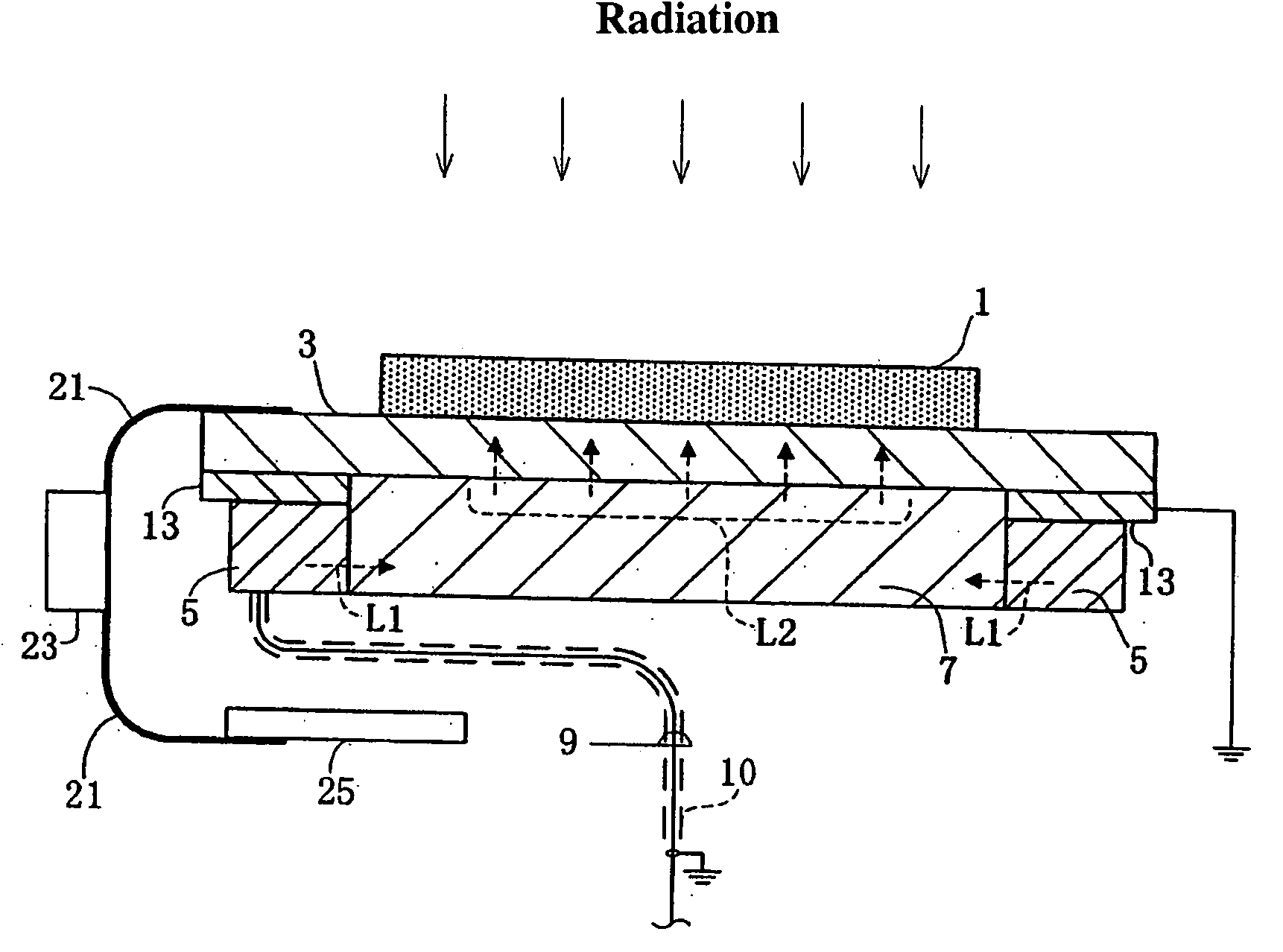
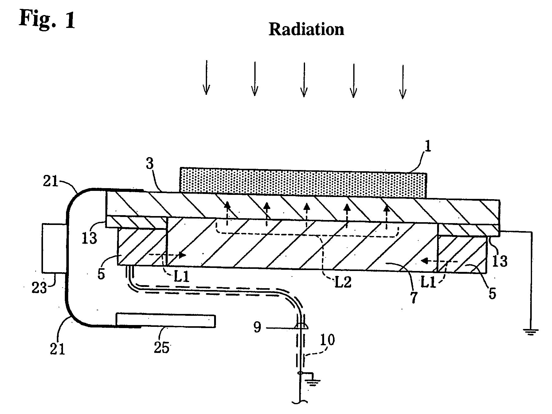
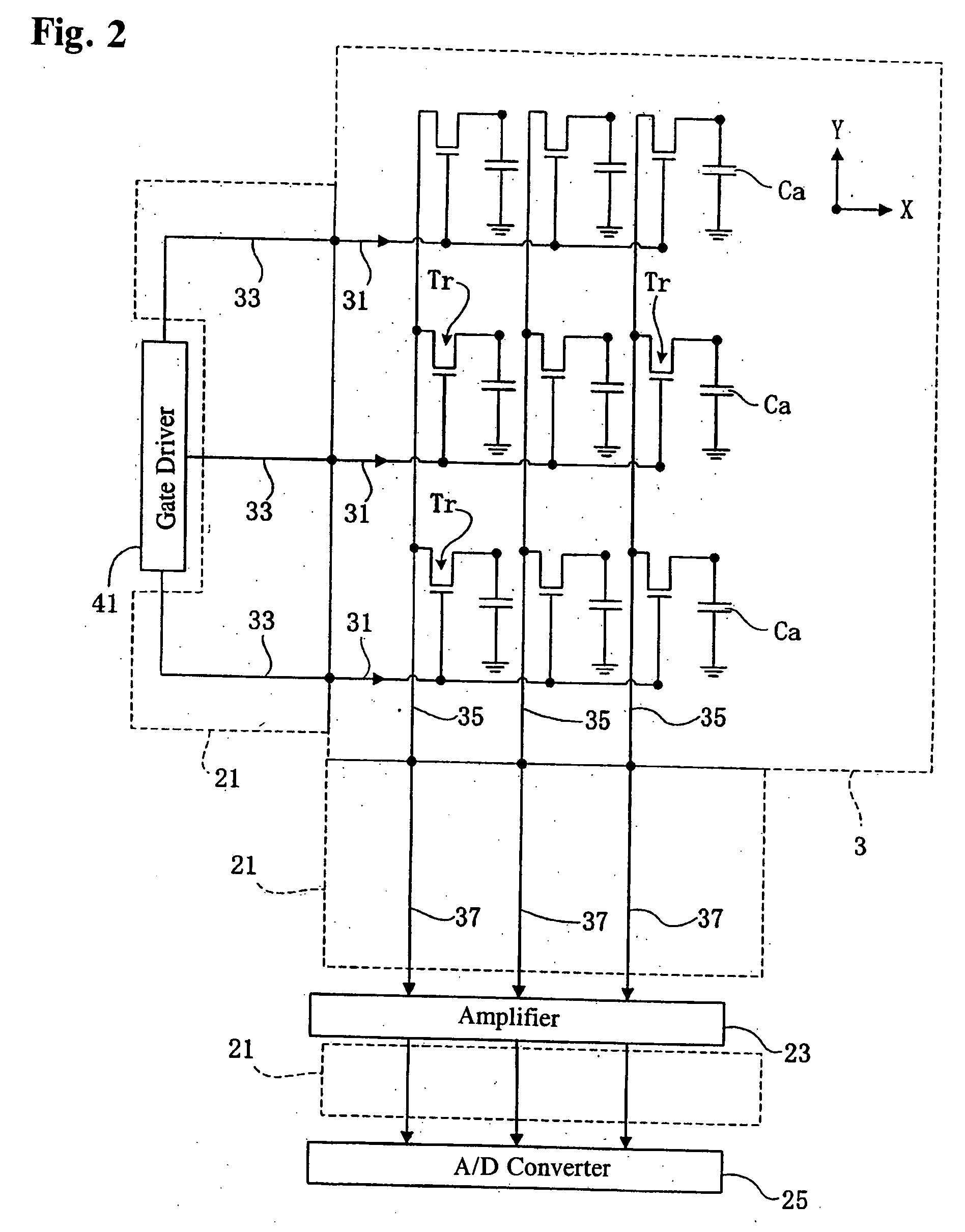
[0033]FIG. 1 is a cross-section showing the structure of a radiation detector according to a first embodiment and FIG. 2 is a simplified circuit diagram of an active matrix substrate, an amplifier and the like and a gate driver.
[0034] The radiation detector according to the first embodiment detects incident radiation to the direction of the solid line arrow as shown in FIG. 1. Radiation is, for example, X-ray and the like. The radiation detector is equipped with a radiation sensitive semiconductor thick film 1 and an active matrix substrate 3 that read out the charge information from the semiconductor thick film 1, wherein the semiconductor thick film 1 is formed on the surface of the active matrix substrate 3. A flat light guide 7 is disposed in the back side of the active matrix substrate 3 with the light emitting face of the flat light guide 7 directed to the active matrix sub...
second embodiment
[0060] Next, the second embodiment of the present invention will be explained. When the composition is the same as the first embodiment, detailed explanations are omitted and the same marks are used.
[0061]FIG. 3 is a simplified drawing showing the structure of a radiation detector according to a second embodiment.
[0062] The radiation detector according to the second embodiment contains an electromagnetic shield 13 that surrounds the light emitting unit 5. An opening is disposed on the electromagnetic shield 13 so that the light emitting unit 5 is allowed to emit light to an end face of the flat light guide 7. Thus, the electromagnetic shield 13, the vertical cross-section of which is shaped like a rectangle without one side, surrounds the light emitting unit 5. The opening, through which the light emitting unit 5 can illuminate, is located at the surface facing the flat light guide 7. Of course the electromagnetic shield 13 of the second embodiment is also made from a conductive m...
PUM
 Abstract
Description
Claims
Application Information
 - R&D
- Intellectual Property
- Life Sciences
- Materials
- Tech Scout
- Unparalleled Data Quality
- Higher Quality Content
- 60% Fewer Hallucinations
Browse by: Latest US Patents, China's latest patents, Technical Efficacy Thesaurus, Application Domain, Technology Topic, Popular Technical Reports.
© 2025 PatSnap. All rights reserved.Legal|Privacy policy|Modern Slavery Act Transparency Statement|Sitemap|About US| Contact US: help@patsnap.com


