
Socket for attaching an electronic component

a technology for attaching electronic components and sockets, which is applied in the direction of coupling contact members, coupling device connections, coupling parts, etc., can solve the problems of increasing the thickness of the perimeter walls of the socket housing, increasing production costs, and difficult to achieve compact design

Inactive Publication Date: 2005-09-29
SMK CORP
View PDF6 Cites 18 Cited by
  • Summary
  • Abstract
  • Description
  • Claims
  • Application Information

AI Technical Summary

Benefits of technology

[0009] In order to overcome the problems of the conventional technology described above, the invention provides an electronic part attachment socket for connecting an electronic part to a printed circuit substrate by way of a plurality of contacts. This includes a socket housing having an electronic part housing section with an open top in which all or part of the electronic part is housed; and a plurality of contacts elastically contacting a terminal of the electronic part. An electronic part attachment socket has a shield case formed in a box shape fitting an outer perimeter of the socket housing in a manner that prevents slipping off. The shield case is formed integrally with an inwardly projecting pushing section. The shield case is fitted to the socket housing in a manner that prevents it from slipping off so that the pushing section pushes the electronic part toward the contacts and the electronic part is supported in the electronic part housing section.
[0012] The electronic part attachment socket of the present invention includes a shield case formed in a box shape fitting an outer perimeter of the socket housing in a manner that prevents slipping off. The shield case is formed integrally with an inwardly projecting pushing section. The shield case is fitted to the socket housing in a manner that prevents it from slipping off so that the pushing section pushes the electronic part toward the contacts and the electronic part is supported in the electronic part housing section. As a result, there is no need to provide a metal securing piece as in the conventional technology, allowing the socket housing to be that much more compact and allowing the overall socket to be compact.
[0013] Also, even if the positioning and outer dimensions of the terminals of electronic parts are the same but the heights are different, compatibility can be maintained simply by changing the shape of the shield case. This makes it possible to share parts such as socket housings and contacts, allowing costs to be kept down.
[0014] By forming the shield case to include a fiat ceiling plate; main side wall plates formed integrally via bends from four sides of the ceiling plate; and secondary side wall plates formed by bending side edges on one side of each of the main side wall plates and forming a section of an adjacent side wall, the need to overlap the shield members at the four corners is eliminated. Thus, the radius of the four corners can be reduced and the overall socket can be made more compact.
[0015] Furthermore, the pushing section is formed by overlapping a pair of push pieces bent from abutted edges of the main side wall plate and the secondary side wall plate. This makes it possible to provide adequate strength for pushing the electronic part.

Problems solved by technology

However, in the conventional technology described above, the installation space needed for the metal securing piece led to an increased thickness in the perimeter walls of the socket housing, making it difficult to achieve a compact design.
Also, even if electronic parts have the same terminal arrangement and outer dimensions, if their heights are different, i.e., the height of the section where the elastic support pieces of the metal securing pieces engage, then it is necessarily to form different metal securing tools, socket housings, and shield members that increases production costs.

Method used


Image

  • Socket for attaching an electronic component
  • Socket for attaching an electronic component
  • Socket for attaching an electronic component

Examples


Embodiment Construction

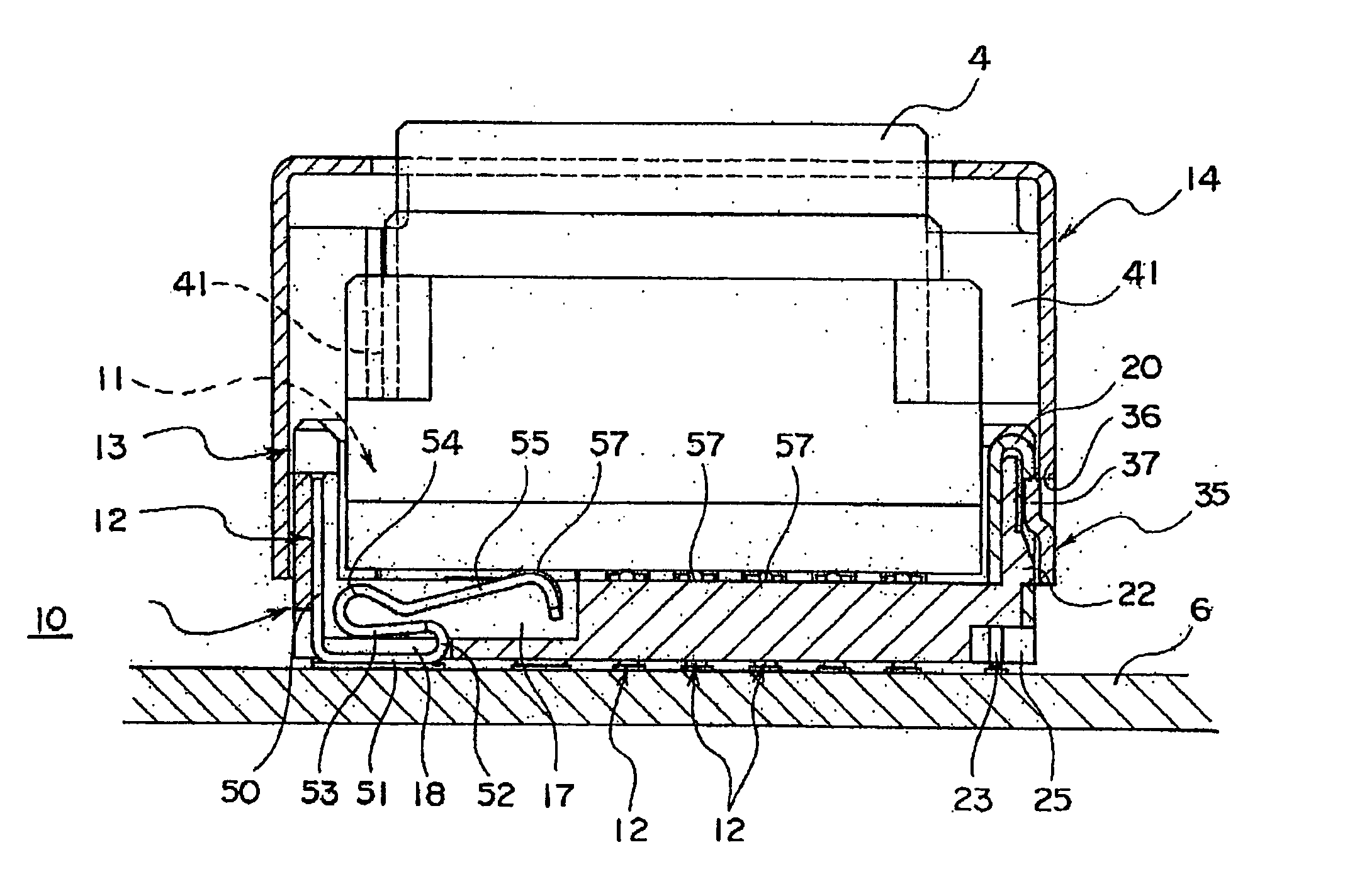
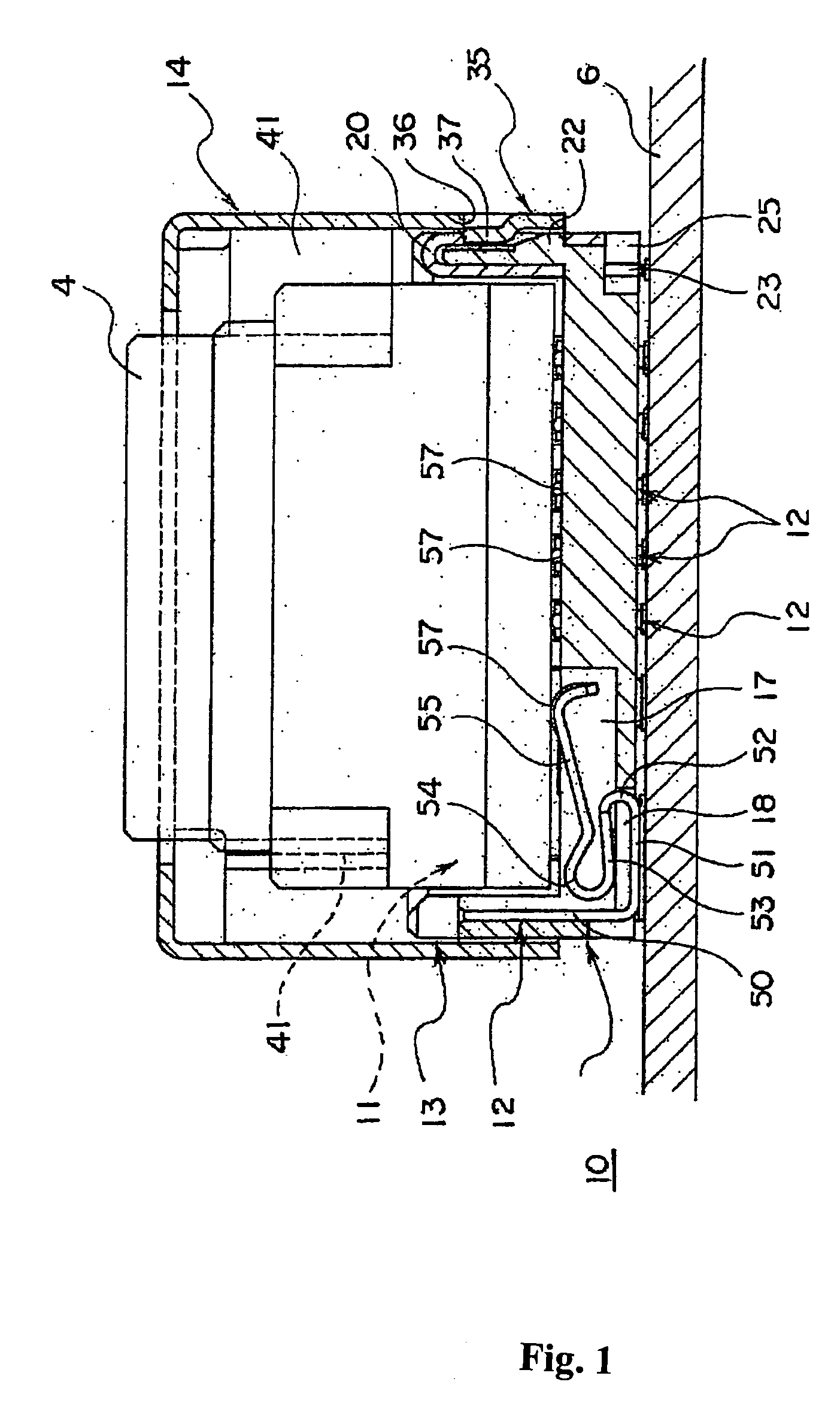
[0037] The electronic part attachment socket according to the present invention will be described using FIG. 1 through FIG. 13. Parts identical to what is described above will be assigned like numerals and corresponding descriptions will be omitted.

[0038]FIG. 1 shows an electronic part such as a camera module being used by being attached to a printed circuit substrate by way of an electronic part attachment socket. The figure shows an electronic part attachment socket 10, a camera module 4, and a printed circuit substrate 6.

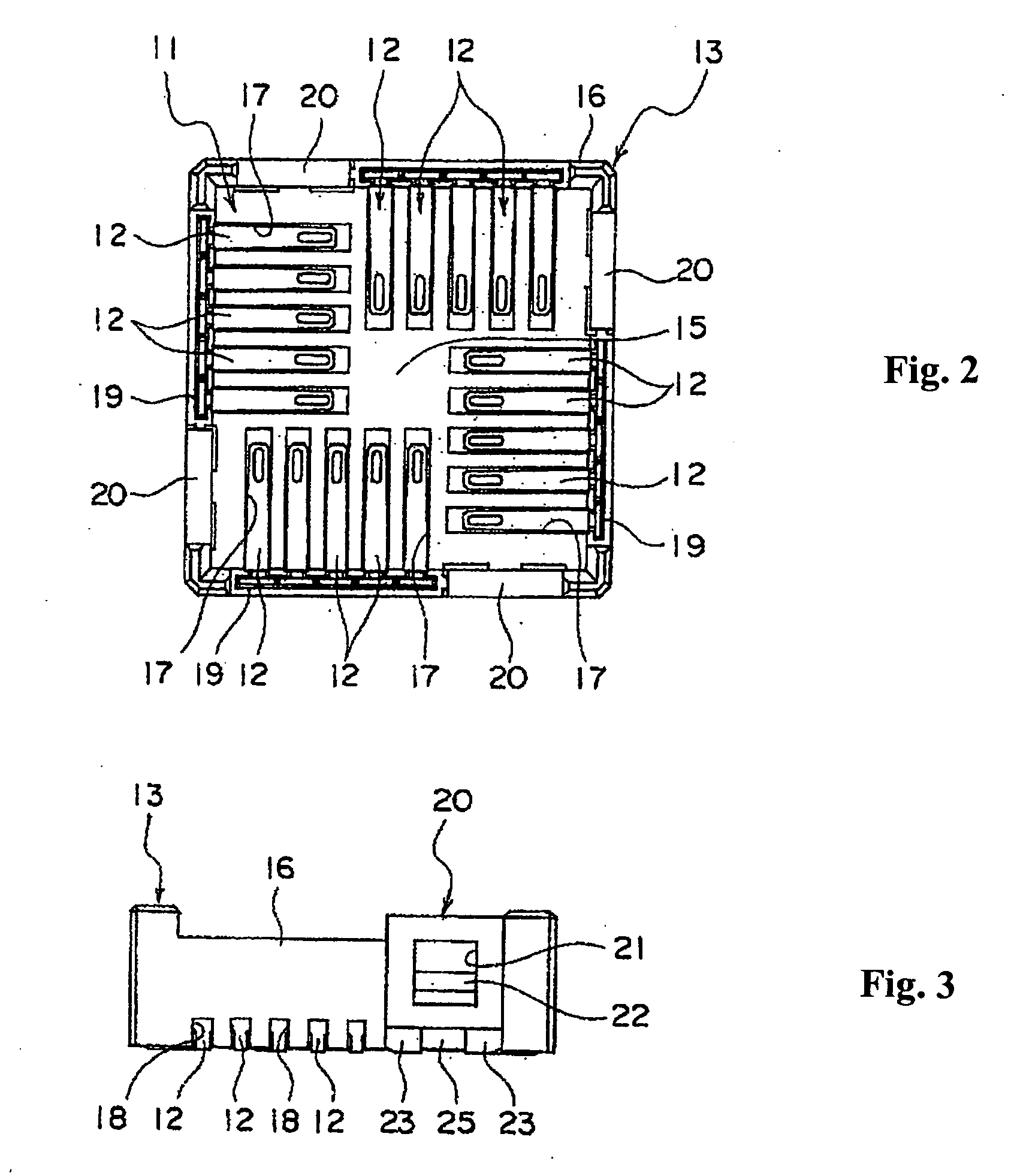
[0039] The electronic part attachment module 10 is equipped with a socket housing 13 including an electronic part housing section 11 with an open upper surface allowing all or part of the electronic part 4 to be housed; and contacts 12, supported by the socket housing 13. The electronic part 4 housed in the electronic part housing section 11 is connected to the printed circuit substrate 6 by way of the contacts 12.

[0040] The electronic part attachment module 1...


PUM


Abstract

An electronic part attachment socket includes a socket housing including an electronic part housing section with an open top into which all or part of an electronic part is housed; and contacts are supported by a socket housing and form an elastic contact with the terminal sections of the electronic part. The electronic part is connected to a printed circuit substrate by way of the contacts. A shield case is formed in a box shape that fits to the outer perimeter of the socket housing, and is formed integrally with a pushing section that projects inward. The shield case is fitted to the socket housing so that it is prevented from slipping off so that the pushing section pushes the electronic part toward the contacts, resulting in the electronic part being housed in the electronic part housing section.

Description

INCORPORATION BY REFERENCE [0001] The present application claims priority under 35 U.S.C. §119 to Japanese Patent Application No. 2004-088388 filed on Mar. 25, 2004. The content of the application is incorporated herein by reference in its entirety. FIELD OF THE INVENTION [0002] The present invention relates to a socket for attaching an electronic part primarily for attaching an electronic part such as a camera modules to a printed circuit substrate. BACKGROUND OF THE INVENTION [0003] Conventionally, in electronic devices such as portable telephones, a printed circuit substrate is installed internally and electronic parts such as camera modules are attached to the printed circuit substrate. Since electronic parts that are heat-sensitive cannot be attached directly with solder, a socket for attaching electronic parts such as shown in FIG. 14 is used for connecting the part to the printed circuit substrate. [0004] The prior art electronic part attachment socket 1 is equipped with a so...

Claims


Application Information

Patent Timeline
IPC IPC(8): H01R13/24H01R13/639H01R13/646H01R13/648H01R33/00H01R33/74H01R33/76
CPCH01R13/24H01R13/6594H01R13/6582H01R12/716H01R13/639
Inventor ASAI, KIYOSHIKANAZAWA, KAZUAKIKOBAYASHI, JUNICHI
Owner SMK CORP
Learn More