Structure and method for ultra-small grain size polysilicon

a polysilicon and grain size technology, applied in semiconductor devices, chemical vapor deposition coatings, coatings, etc., can solve the problems of large resistance, increased polysilicon, and increased resistance, and achieve the effect of reducing polysilicon depletion and facilitating dopant diffusion

Inactive Publication Date: 2005-06-16
IBM CORP
View PDF5 Cites 3 Cited by
  • Summary
  • Abstract
  • Description
  • Claims
  • Application Information

AI Technical Summary

Benefits of technology

[0021] The present inventors have recognized that breaking the polysilicon film into two parts (e.g., first and second layers) where the first polysilicon layer sets the polysilicon grain size, is very advantageous in achieving such ultra small polysilicon grain size.
[0022] There are many advantages of the present invention including that it is very simple and inexpensive to integrate the present invention into the process. Additionally, the invention is applicable to any substrate, bulk or silicon-on-insulator (SOI), SiGe, etc.
[0024] Further, the small grain size facilitates dopant diffusion and reduces polysilicon depletion.

Problems solved by technology

However, this 50 nm grain size creates many problems including that the polysilicon is more bamboo-like along the gate lines, and conductivity / resistivity becomes more sensitive to grain size at this nano-scale level (e.g., conductivity / resistivity tracks with grain size).
This is problematic because the resistance would be very large otherwise.
Another problem is that the diffusion of dopants in these “large-grain” polysilicon gates will probably be mostly through lattice diffusion (similar to that of crystalline silicon) which is relatively slow (e.g., typically about a factor of 10 slower than diffusion for polysilicon) and sufficient dopant may not reach the polysilicon / oxide interface, where dopant is also needed to prevent polysilicon depletion effects.
Further, one may have to increase thermal budgets enormously (e.g., to 1050° C. for about 5 seconds or the like, depending upon the dopants used, etc.) to cause dopants to reach the polysilicon / oxide interface and recoup this depletion loss, which then impacts channel doping adversely.
That is, it is well known that polycrystalline grain size may somewhat correlate with film thickness, and given that the typical gate stack thicknesses are in the 100 nm range, it is difficult to limit the grain size to the 10-20 nm range.

Method used


Image

  • Structure and method for ultra-small grain size polysilicon
  • Structure and method for ultra-small grain size polysilicon
  • Structure and method for ultra-small grain size polysilicon

Examples


second embodiment

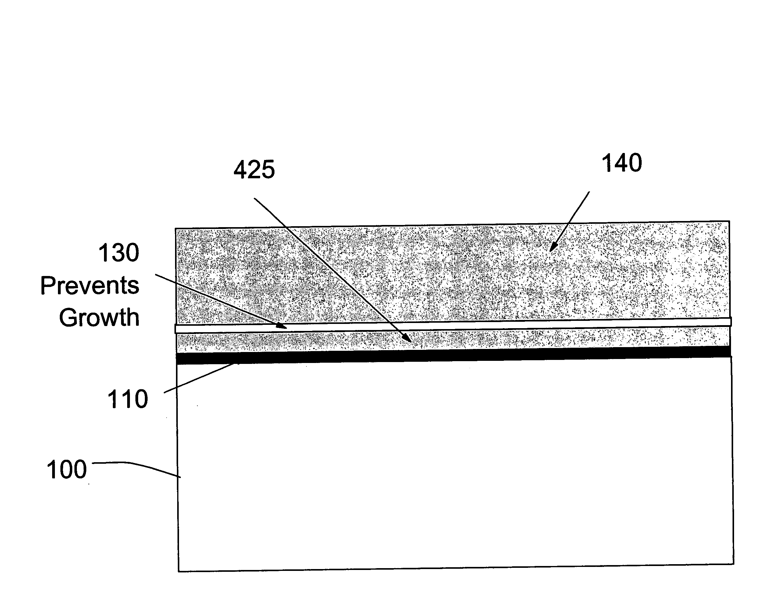
[0048] Turning to FIG. 4, a second embodiment of the inventive method is shown.

[0049] Specifically, FIG. 4 illustrates a gate stack formed by the second embodiment in which the small grained polysilicon 125 of the first embodiment is replaced by a small-grained SiGe layer 425. In addition to the advantages of the first embodiment, this SiGe layer provides the additional advantage of better activation of the dopants (e.g., see Ozturk et al., International Workshop on Junction Technology, 2001, page 77).

[0050] More specifically, alternatively to the amorphous Si or the polysilicon for the first layer 125 in the first embodiment, the second embodiment of the present invention recognizes that it is also advantageous if SiGe is used for the thin layer 125. That is, SiGe is known to have better dopant activation than the small grained polysilicon, and the activation could be even higher for ultra-small (e.g., approximately 10-20 nm) grain poly-SiGe.

[0051] Hence, as shown in FIG. 4, the...


PUM

PropertyMeasurementUnit
grain sizeaaaaaaaaaa
thicknessaaaaaaaaaa
temperatureaaaaaaaaaa

Abstract

A method of forming a semiconductor structure (and the resulting structure), includes providing a nitride layer between a silicon-containing layer and a polysilicon layer.

Description

BACKGROUND OF THE INVENTION [0001] 1. Field of the Invention [0002] The present invention generally relates to a semiconductor device and method therefor, and more particularly to a structure and method of ultra-small (e.g., within a range of about 10 nm to about 20 nm) grain size polysilicon. [0003] 2. Description of the Related Art [0004] State-of-the-art complementary metal oxide semiconductor (CMOS) gates are beginning to target 30 nm lengths. Typical polysilicon grain sizes are in the 50 nm range (e.g., see S. Wolf, Silicon Processing for the VLSI Era, Vol. 2, Lattice Press, 1990; U.S. Pat. No. 6,294,442). [0005] However, this 50 nm grain size creates many problems including that the polysilicon is more bamboo-like along the gate lines, and conductivity / resistivity becomes more sensitive to grain size at this nano-scale level (e.g., conductivity / resistivity tracks with grain size). [0006] More specifically, assume that one has a 30 nm grain size and a 30 nm gate polysilicon is ...

Claims


Application Information

Patent Timeline
Patent Type & Authority Applications(United States)
IPC IPC(8): C23C16/02C23C16/24H01L21/20H01L21/205H01L21/28H01L21/3205H01L29/49
CPCC23C16/0272C23C16/24H01L21/28035H01L21/02532H01L29/4925H01L21/02381H01L21/02488H01L21/32055
Inventor BEINTNER, JOCHENCHIDAMBARRAO, DURESETI
Owner IBM CORP
Why Eureka
Try Eureka