
LED curing apparatus and method

a curing apparatus and curing system technology, applied in the field of curing apparatus, system and method, can solve the problems of shortening the emission wavelength, requiring the use of expensive and complicated heat transfer systems, and reducing the irradiance and lifetime quickly

Inactive Publication Date: 2005-06-02
3M INNOVATIVE PROPERTIES CO
View PDF71 Cites 76 Cited by
  • Summary
  • Abstract
  • Description
  • Claims
  • Application Information

AI Technical Summary

Benefits of technology

The present invention is a radiation curing apparatus that uses solid state radiation sources, such as LED dies or laser diodes, and optical concentrators to generate curing radiation. The concentrators receive the radiation from the sources and transmit it through optical waveguides to a substrate where the curing chemical formulation is exposed. The technical effects of this invention include higher efficiency in generating curing radiation, improved control over the radiation's wavelength and direction, and reduced energy consumption.

Problems solved by technology

In addition, expensive and complicated heat transfer systems must be employed if heat is to be removed from the area of illumination.
With these conventional systems, however, the irradiance and lifetime drop quickly as the LED emission wavelengths get shorter.
This may lead to problems with initiating chemical reactions via radiation absorption and response by photoinitiators, which are typically formulated to absorb radiation less than 450 nm.
If the irradiance is too low, it is possible that the polymerization reaction would not yield desired product properties.
However, arranging the LEDs in such a manner results in several complications relating to thermal management and electrical connections.
If the LEDs are more spread out, irradiance uniformity across the array can become non-ideal.
Reflectors are sometimes mounted around the LEDs to improve irradiance levels, but this approach still suffers from non-uniformity across the reflector opening.

Method used


Image

  • LED curing apparatus and method
  • LED curing apparatus and method
  • LED curing apparatus and method

Examples


Embodiment Construction

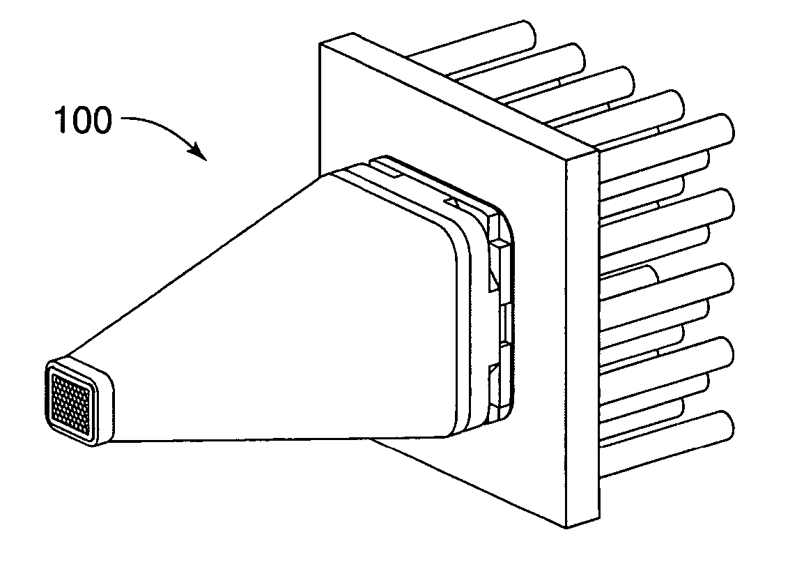
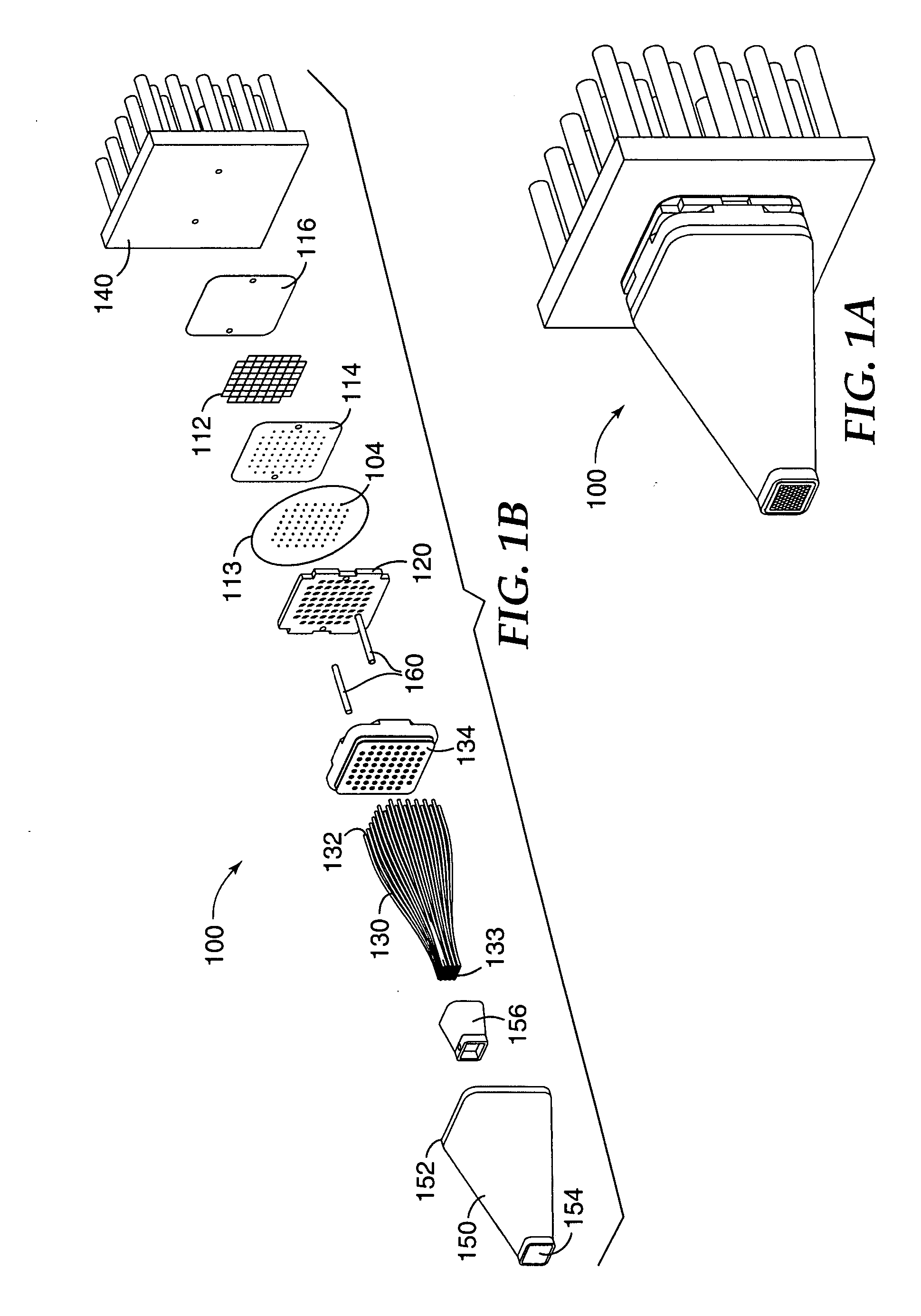
[0030]FIG. 1A shows a solid state light device 100 (also referred to herein as an illumination device or photon emitting device) in an exemplary configuration. Light device 100 is shown in an exploded view in FIG. 1B. By “light” it is meant electromagnetic radiation having a wavelength in the ultraviolet, visible, and / or infrared portion of the electromagnetic spectrum. In the construction described below, the light device 100 can have an overall compact size comparable to that of a conventional High Intensity Discharge (HID) bulb, thus providing a replacement for a discharge lamp device in various applications including road illumination, spot lighting, back lighting, image projection and radiation activated curing.

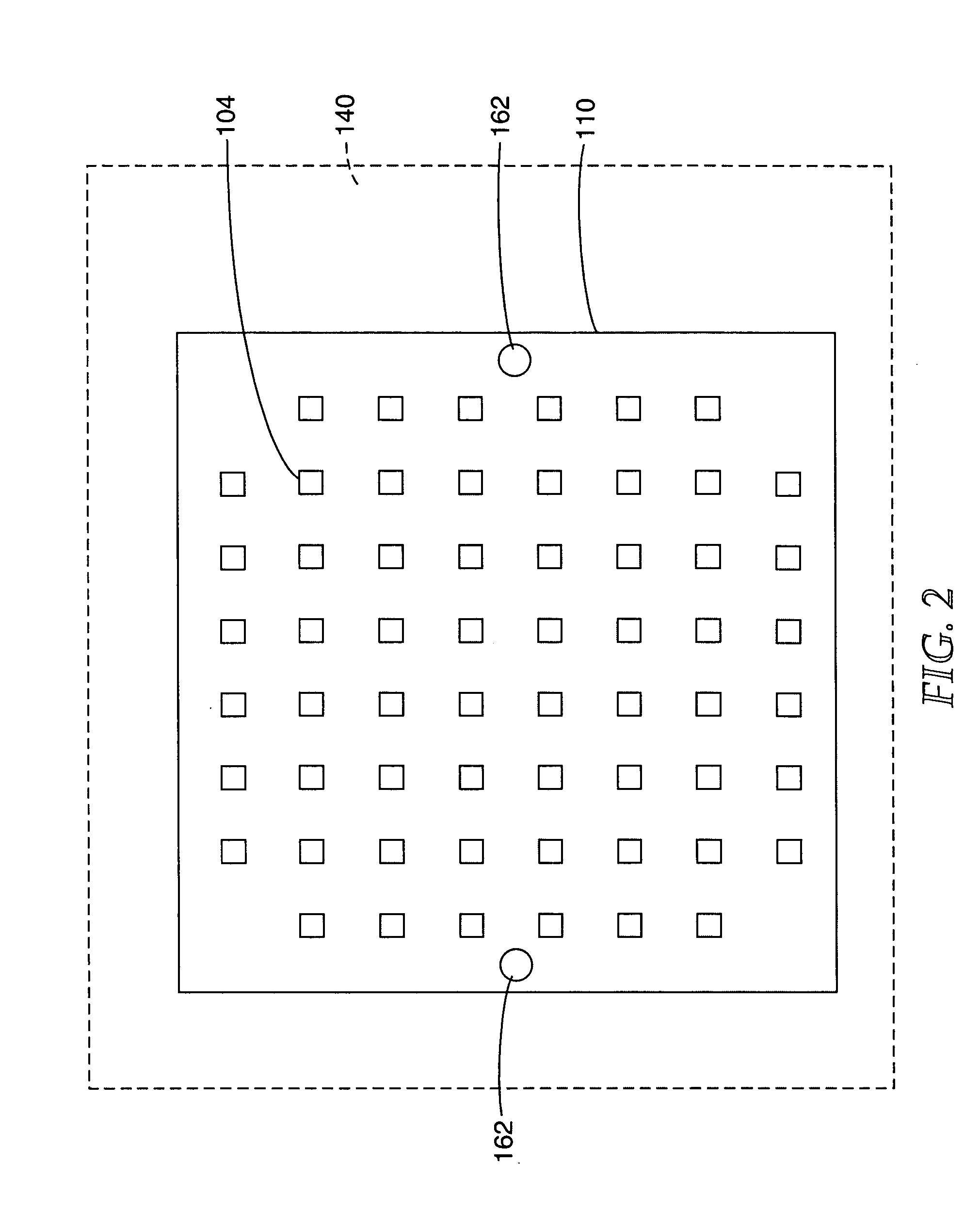
[0031] Light device 100 comprises an array of solid state radiation sources 104 to generate radiation. The radiation is collected and concentrated by a corresponding array of optical concentrators 120. The concentrated radiation is then launched into a corresponding arr...


PUM


Abstract

A radiation curing apparatus comprises a plurality of solid state radiation sources to generate radiation that cures a first material. The solid state radiation sources can be disposed in an array pattern. Optical concentrators, arranged in a corresponding array pattern, receive radiation from corresponding solid state radiation sources. The concentrated radiation is received by a plurality of optical waveguides, also arranged in a corresponding array pattern. Each optical waveguide includes a first end to receive the radiation and a second end to output the radiation. The curing apparatus can be utilized for continuous substrate, sheet, piece part, spot curing, and / or 3D radiation-cure processes.

Description

RELATED APPLICATION [0001] The present application is related to co-owned and concurrently filed U.S. patent application entitled “Solid State Light Device” (Atty. Docket No. 59349US002), incorporated by reference herein in its entirety. The present application is also related to co-owned and concurrently filed U.S. Patent applications entitled “Reflective Light Coupler” (Atty. Docket No. 59121US002); “Illumination System Using a Plurality of Light Sources” (Atty. Docket No. 58130US004); “Multiple LED Source and Method for Assembling Same” (Atty. Docket No. 59376US002); “Illumination Assembly” (Atty. Docket No. 59333US002), “Phosphor Based Light Sources Having a Polymeric Long Pass Reflector” (Atty. Docket No. 58389US004); and “Phosphor Based Light Sources Having a Non-Planar Long Pass Reflector” (Atty. Docket No. 59416US002) each of which is incorporated by reference herein in its entirety.BACKGROUND OF THE INVENTION [0002] 1. Field of the Invention [0003] The present invention rel...

Claims


Application Information

Patent Timeline
Patent Type & Authority Applications(United States)
IPC IPC(8): A61C13/15A61C19/00F21K99/00G02B6/06G02B6/42
CPCA61C19/003A61C19/004F21K9/00G02B6/06G02B6/4201F21V29/80G02B6/423G02B6/4231G02B6/4249G02B6/4298G02B6/4206G02B6/4269F21K9/69
Inventor AGUIRRE, FRANCIS M.CRATON, MICHELE A.LAI, JACK W.PHILLIPS, DAVID L.BENSON, PETER T.HENSON, GORDON D.MEIS, MICHAEL A.
Owner 3M INNOVATIVE PROPERTIES CO
Learn More