
Fabrication of nanoscale thermoelectric devices

Inactive Publication Date: 2005-05-26
CANON KK
View PDF23 Cites 76 Cited by
  • Summary
  • Abstract
  • Description
  • Claims
  • Application Information

AI Technical Summary

Benefits of technology

[0017] Also, it is preferred that the p-type nanowires and the n-type nanowires are interspersed among each other for easier thermocouple formation. The nanowires may be interspersed in a comb-like arrangement by patterning the first bottom electrode pattern such that the first group of bottom electrodes and the second group of bottom electrodes alternate spatially.
[0020] Because holes are formed in the substrate to replace the first bottom electrode pattern, portions of the substrate are left intact, thereby avoiding removal of the entire substrate. Consequently, the substrate's structural integrity is maintained and the substrate may continue to provide support for the device. This support is especially beneficial since nanoscale structures, in particular these nanowires, are fragile in comparison to bulk structures. In addition, the substrate not only acts as a support structure but also may shield the nanowires from physical impact during device manufacture.
[0021] Preferably, the holes which are formed in the substrate have a keystone shape. The keystone shape is seen to provide two benefits. First, the keystone shape allows for a more even deposition of electrode materials. This is of benefit with respect to the second set of holes in which new connections are to be formed. Second, the keystone shape requires a less fine pattern for proper hole placement. This is due to the shape of the keystone, which is wider at the base than at the top. Formation of the base may be less fine, since the shape naturally narrows as it bores into the substrate. To achieve the keystone shape, potassium hydroxide is preferably used to etch the substrate.

Problems solved by technology

However, since the relationship between electrical conductivity and thermal conductivity for metals is fixed, the research yielded limited success.
However, nanoscale elements are not easily produced by conventional methods.
This is difficult for nanowires and their small diameters because increased length would increase the fragility of the nanowires.
Conventional methods typically would not meet tolerances required for the production of nanowire thermoelectric modules and would likely damage their fragile structures.

Method used


Image

  • Fabrication of nanoscale thermoelectric devices
  • Fabrication of nanoscale thermoelectric devices
  • Fabrication of nanoscale thermoelectric devices

Examples


Embodiment Construction

[0037] The present invention provides a method for fabricating a nanoscale thermoelectric module (TEM), wherein the thermoelements are nanowire structures. The TEM produced is expected to have more efficient thermoelectric qualities due to the nanowire thermoelements. Furthermore, the fabrication method that is likely to yield numerous advantages, such as a decreased likelihood of damage to the nanowires during device fabrication, adaptability to automation, and lower manufacturing costs.

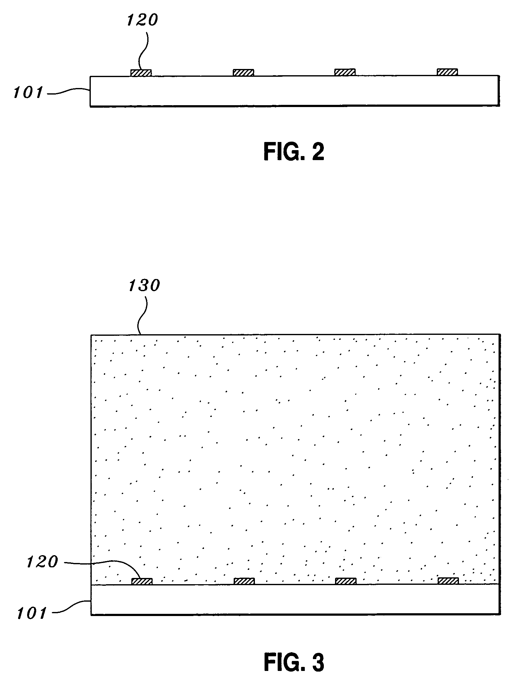
[0038] In one aspect of the present invention, a substrate is provided upon which a first bottom electrode pattern is disposed. FIG. 1 is an elevated view of the top surface of an exemplary substrate (101) with a first bottom electrode pattern (105) disposed thereon, wherein the first bottom electrode pattern has a first electrically connected group of bottom electrodes; a second electrically connected group of bottom electrodes; and a first set of connections.

[0039]FIG. 2 shows a cross-sectional ...


PUM


Abstract

In a method for fabricating a nanowire thermoelectric device, a first electrode pattern is formed on a substrate, wherein the first electrode pattern includes bottom electrodes and a first set of connections which connects the bottom electrodes to form first and second groups of electrically connected bottom electrodes. P-type nanowires and n-type nanowires are selectively formed on the substrate by selectively activating either the first group of electrically connected bottom electrodes and the second group. The p-type and n-type nanowires are then connected by top electrodes. A first set of holes in the substrate is formed to remove the first set of connections. A second set of holes to allow for electrical access to the bottom electrodes, and a second set of connections are formed, so as to result in an array of thermocouples connected to each other in parallel banks of series-connected thermocouples.

Description

BACKGROUND AND SUMMARY [0001] 1. Field of the Invention [0002] The present invention generally relates to a method for fabricating nanowire thermoelectric devices. [0003] 2. Description of the Related Art [0004] Nanowires are known in the art as wire structures which have a diameter measured in hundreds of nanometers (nm) or less, typically measured from 1 to 500 nm. When devices are constructed using structures of such a small scale, quantum mechanical rules and phenomena begin to have a greater effect on the operation of such devices in comparison to larger scale structures. The increased role and effect of quantum mechanics is due to the reduced number of atoms and electrons present in the system, which makes their discrete quantum natures more apparent. [0005] While it is not known how quantum mechanics will affect the operation of all nanoscale devices, it has been found that thermoelectric modules (TEMs) constructed using nanowires are likely to show increased efficiency relat...

Claims


Application Information

Patent Timeline
IPC IPC(8): H01L21/44H01L35/32H01L35/34
CPCH01L35/32Y10S977/833H01L35/34H10N10/01H10N10/17
Inventor OKAMURA, YOSHIMASAKOHLER, TIMOTHY L.
Owner CANON KK
Learn More