
Ceramic end effector for micro circuit manufacturing

a technology of end effector and micro-circuit, which is applied in the direction of program-controlled manipulators, thin material processing, article separation, etc., can solve the problems of metal contamination within the processing chamber, high temperature of the thermal process, so as to achieve low cost

Inactive Publication Date: 2005-05-26
AXCELIS TECHNOLOGIES
View PDF35 Cites 55 Cited by
  • Summary
  • Abstract
  • Description
  • Claims
  • Application Information

AI Technical Summary

Benefits of technology

[0006] A ceramic end effector with an interior passage for vacuum provides relatively low cost, lightweight, and contaminate free wafer handling for high temperature thermal processing applications.
[0008] The support pads are secured to the end effector utilizing a unique spring which through its action forces the support pad in a downward direction against the body portion. The spring additionally forces that pad forward against an angled surface on the body. The pad is thus forced downward and into contact with the body at the angled interface as well. The surface of the bottom of the pad and that of the mating surface of the body are ground to a high degree of flatness to effect a seal that has very low leakage. The pad and body in this configuration may expand or contract at different rates as well as move relative to each other without affecting the seal or introducing stressed into either component. The underside of the vacuum pad features a counterbore which when exposed to negative pressure results in a net downward force against the end effector body thus improving the effectiveness of the seal between the pad and the end effector body. The pads are conveniently removable and / or replaceable in the event of damage or contamination.

Problems solved by technology

Many of these thermal processes involve extremely high temperatures.
One source of contamination that is detrimental to thermal processes is metal.
Some vacuum type end effectors have metal components such as vacuum lines that make them susceptible to metal contamination within the processing chamber.
Some existing vacuum type end effectors have plastic components such as wafer support pads that are not suitable for high temperature thermal processes because they would melt on contact with the heated wafer.

Method used


Image

  • Ceramic end effector for micro circuit manufacturing
  • Ceramic end effector for micro circuit manufacturing
  • Ceramic end effector for micro circuit manufacturing

Examples


Embodiment Construction

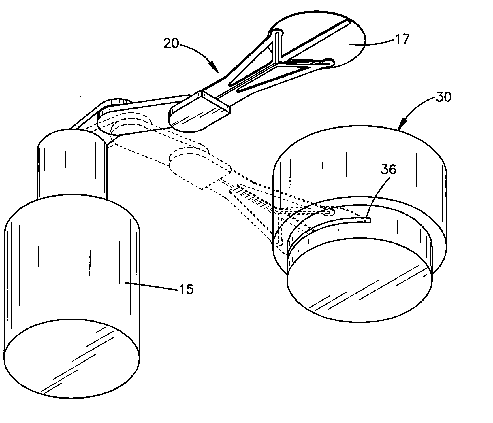
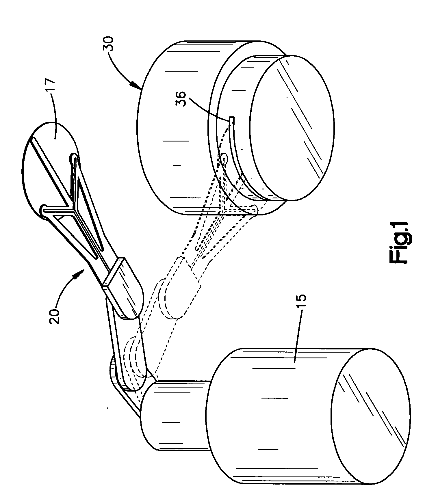
[0021]FIG. 1 shows an overview of an end effector 20 installed on a typical wafer handling robot 15 that is loading an RTP machine 30. The end effector 20 grips a wafer 17 and installs it through a slot 36 into the RTP processing chamber. Upon completion of the thermal process, the end effector is inserted into the processing chamber and retrieves the wafer 17 for transport to the next step in fabrication.

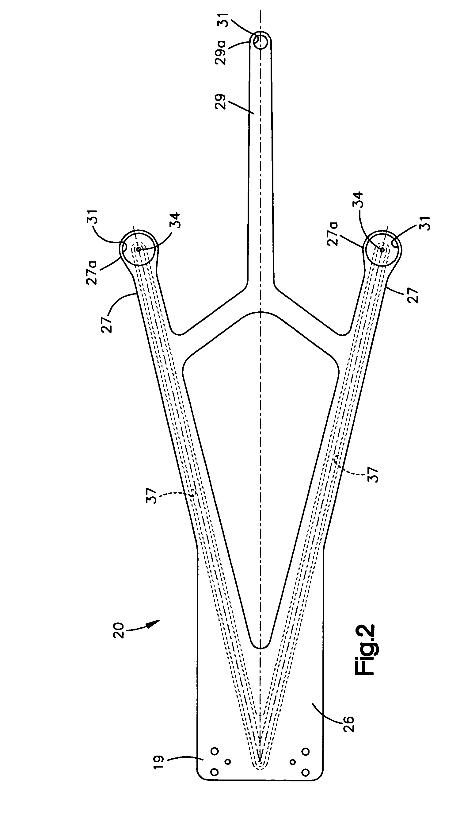
[0022]FIGS. 2-6 show the end effector 20 according to the present invention in more detail. The end effector 20 includes a body portion 25 that is made of a ceramic material such as, alumina, or silicon carbide, but preferably alumina. The body portion 25 is generally planar in shape and features a robot arm mounting end 19, and two outer wafer engaging fingers 27 and a center wafer support finger 29 at an axial end. The outer wafer engaging fingers 27 and support 29 each have a wafer support pad cavity which houses a wafer support pad that support the wafer during handling withou...


PUM


Abstract

An end effector for installation on a robotic arm for transporting a plurality of semiconductor wafers from one location to another features a ceramic end effector body portion that includes a plurality of wafer engaging fingers that each feature wafer support pads. The wafer support pads are adapted to support a semiconductor wafer surface, and at least one of the support pads has a vacuum orifice. The pads are replaceable and / or removable in case of damage or contamination. The support pads are attached to the body in such a way as to allow differential thermal expansion so as to prevent introduction of stress into the components. Typically, a wire spring is employed to secure the pad to the end effector. The body portion features an interior vacuum passageway having a first end that is adapted to connect to a vacuum source and a second end that terminates at the vacuum orifices such that a reduced gas pressure at the first end causes a vacuum to be exerted at the vacuum orifices. The interior passageway is formed from a groove in the end effector body portion and an end effector backplate that is sealingly connected to the end effector body portion to completely cover the groove from the first end to the second end. The ceramic body portion can be made of alumina or silicon carbide.

Description

RELATED APPLICATION [0001] The present application is a continuation-in-part application of U.S. application Ser. No. 10 / 305,731, filed Nov. 26, 2002 and entitled CERAMIC END EFFECTOR FOR MICRO CIRCUIT MANUFACTURING.TECHNICAL FIELD [0002] The present invention relates generally to semiconductor wafer processing and more specifically to an end effector for handling semiconductor wafers during processing. BACKGROUND OF THE INVENTION [0003] Thermal processing systems are widely used in various stages of semiconductor fabrication. Basic thermal processing applications include chemical deposition, diffusion, oxidation, annealing, silicidation, nitridation, and solder re-flow processes. Many of these thermal processes involve extremely high temperatures. For example, vertical rapid thermal processing (RTP) systems comprise a vertically oriented processing chamber that is heated by a heat source such as a resistive heating element or a bank of high intensity light sources. The heat source ...

Claims


Application Information

Patent Timeline
IPC IPC(8): B25J9/00B25J15/06H01L21/683
CPCB25J9/0012H01L21/6838B25J15/0616
Inventor BAUMANN, PAUL W.DEAK, MIHALY IVPHARAND, MICHELPOLNER, DONALD N.
Owner AXCELIS TECHNOLOGIES
Learn More