
Plasma display panel driver, driving method thereof, and plasma display device

a technology of plasma display panel and driver, which is applied in the direction of identification means, instruments, light sources, etc., can solve the problems of poor efficiency and conventional power recovery circuits that fail to recover 100% of reactive power during the power recovery process, and achieve the effect of reducing the amount of capacitive load

Inactive Publication Date: 2005-04-07
SAMSUNG SDI CO LTD
View PDF2 Cites 17 Cited by
  • Summary
  • Abstract
  • Description
  • Claims
  • Application Information

AI Technical Summary

Benefits of technology

[0050] The discharge amount of the capacitive load is reduced when a predetermined number of second electrodes are continuously selected in the selecting circuit while the first electrodes are sequentially selected.

Problems solved by technology

Conventional power recovery circuits fail to recover 100% of the reactive power during the power recovery process due to switching losses in the transistors or parasitic components of the circuit.
As a result, the power recovery operation cannot set the voltage at the panel capacitor to a desired voltage, and the switch must perform hard switching.
The conventional power recovery circuit continues to perform power recovery in this case, even though power recovery is not necessary, thereby worsening efficiency.

Method used


Image

  • Plasma display panel driver, driving method thereof, and plasma display device
  • Plasma display panel driver, driving method thereof, and plasma display device
  • Plasma display panel driver, driving method thereof, and plasma display device

Examples


Embodiment Construction

[0065] In the following detailed description, only exemplary embodiment of the invention has been shown and described, simply illustrating the best mode contemplated by the inventor(s) of carrying out the invention. As will be realized, the invention is capable of modification in various obvious respects, all without departing from the spirit of the invention. Accordingly, the drawings and description are to be regarded as illustrative in nature, and not restrictive.

[0066] A plasma display device, a PDP driver, and a PDP driving method will be described in detail with reference to the drawings.

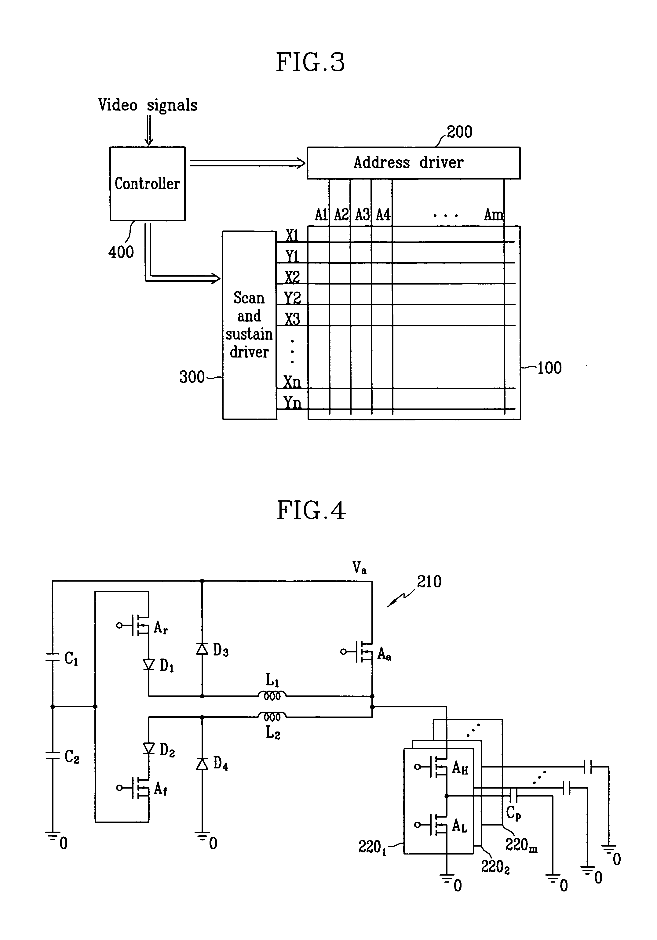
[0067]FIG. 3 shows a brief diagram of a plasma display device according to a preferred embodiment of the present invention.

[0068] As shown, the plasma display device comprises a PDP 100, an address driver 200, a scan and sustain driver 300, and a controller 400. The scan and sustain driver 300 is illustrated as a single block in FIG. 3, but it can also be separated into a scan driver and a ...


PUM


Abstract

In an address driving circuit including a power recovery circuit, an energy charged in an external capacitor is established to be greater than an energy discharged from the external capacitor. As a result, a voltage of the external capacitor is increased to an address voltage to automatically stop a power recovery operation in the case of displaying a full white pattern. Further, to perform the power recovery operation in the cases of the dot on / off pattern and the line on / off pattern, the voltage of the external capacitor reaches an equilibrium state between the half the address voltage and the address voltage.

Description

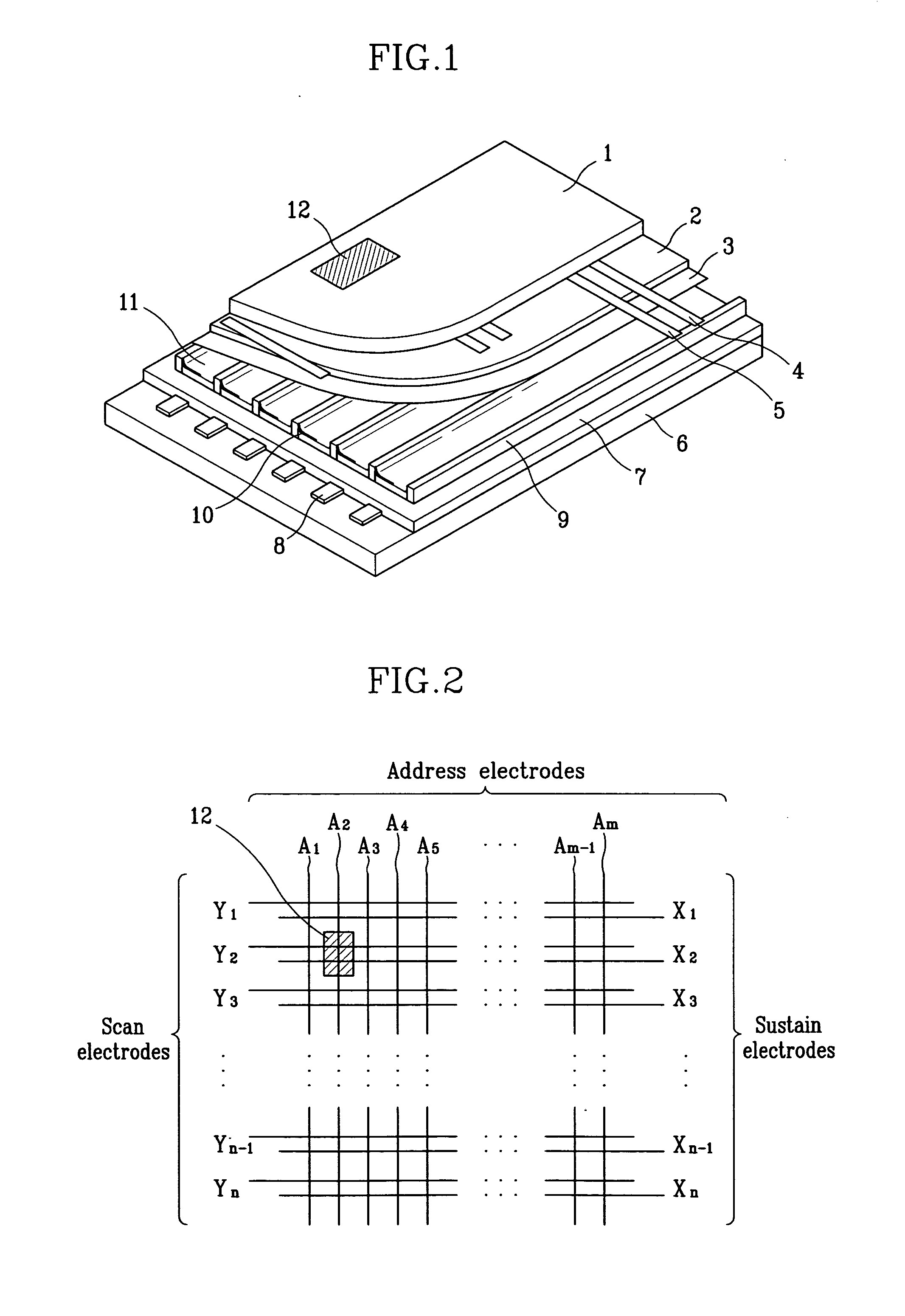
CROSS REFERENCE TO RELATED APPLICATION [0001] This application claims priority to and the benefit of Korea Patent Application No. 2003-69126, filed on Oct. 6, 2003, in the Korean Intellectual Property Office, the content of which is incorporated herein by reference. BACKGROUND OF THE INVENTION [0002] (a) Field of the Invention [0003] The present invention relates to a plasma display panel (PDP) driving circuit. More specifically, the present invention relates to an address driving circuit for applying address voltages. [0004] (b) Description of the Related Art [0005] The PDP is a flat display that uses plasma generated via a gas discharge process to display characters or images, and, depending on its size, tens to millions of pixels are provided thereon in a matrix format PDPs are categorized as direct current (DC) PDPs or alternating current (AC) PDPs according to the supplied driving voltage waveforms and discharge cell structures. [0006] DC PDPs have electrodes exposed in the dis...

Claims


Application Information

Patent Timeline
IPC IPC(8): G09G3/20G09F9/313G09G3/288G09G3/291G09G3/293G09G3/296G09G3/298H01J17/49H05B41/16
CPCG09G3/2965G09G3/293G09G3/296
Inventor LEE, JUN-YOUNGAN, BYUNG-NAMJUNG, NAM-SUNG
Owner SAMSUNG SDI CO LTD
Learn More