
Multi-layered metal routing technique

a metal routing and multi-layer technology, applied in the direction of semiconductor devices, semiconductor/solid-state device details, electrical devices, etc., can solve the problem of inability to interconnect higher layers of metal

Active Publication Date: 2005-03-17
TAIWAN SEMICON MFG CO LTD
View PDF12 Cites 2 Cited by
  • Summary
  • Abstract
  • Description
  • Claims
  • Application Information

AI Technical Summary

Benefits of technology

[0014] A principal objective of the invention is to provide a method of creating overlying layers of interconnect metal that do not negatively affect device performance and device reliability.

Problems solved by technology

This would make it impossible to interconnect higher layers of metal if these layers do not need to be connected to a first layer of metal.

Method used


Image

  • Multi-layered metal routing technique
  • Multi-layered metal routing technique
  • Multi-layered metal routing technique

Examples


Embodiment Construction

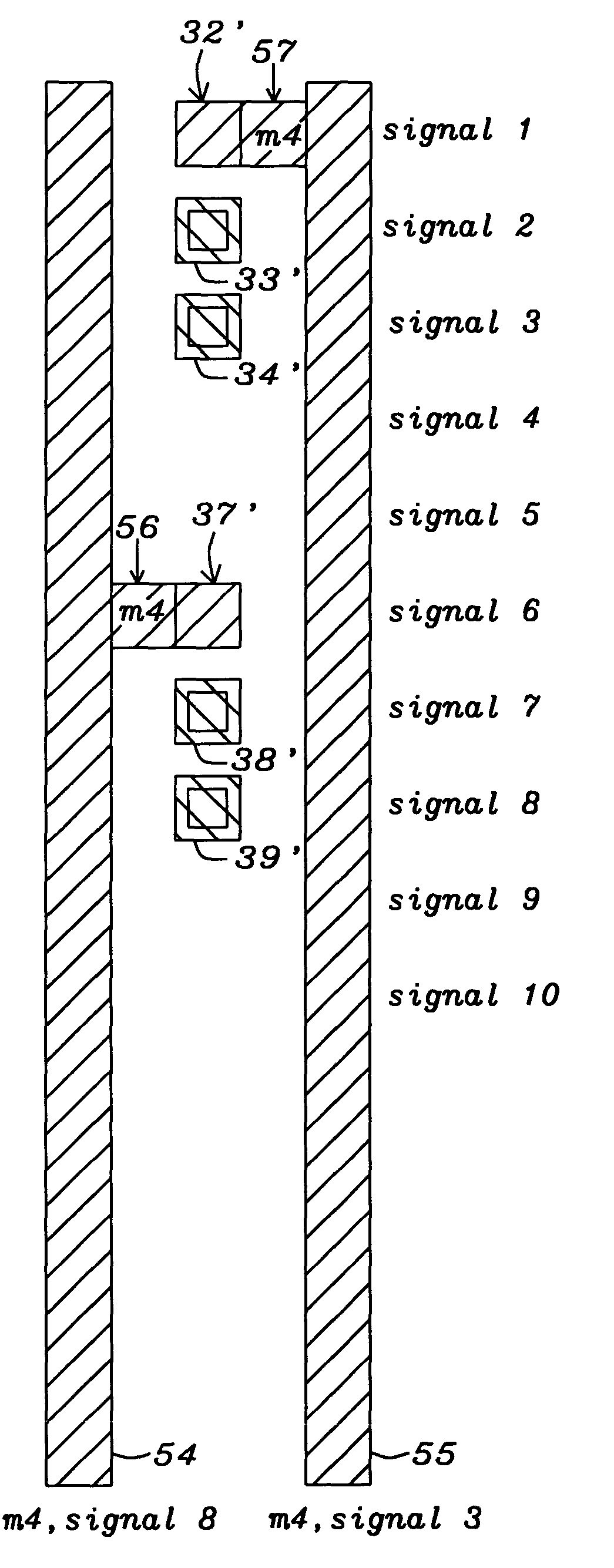
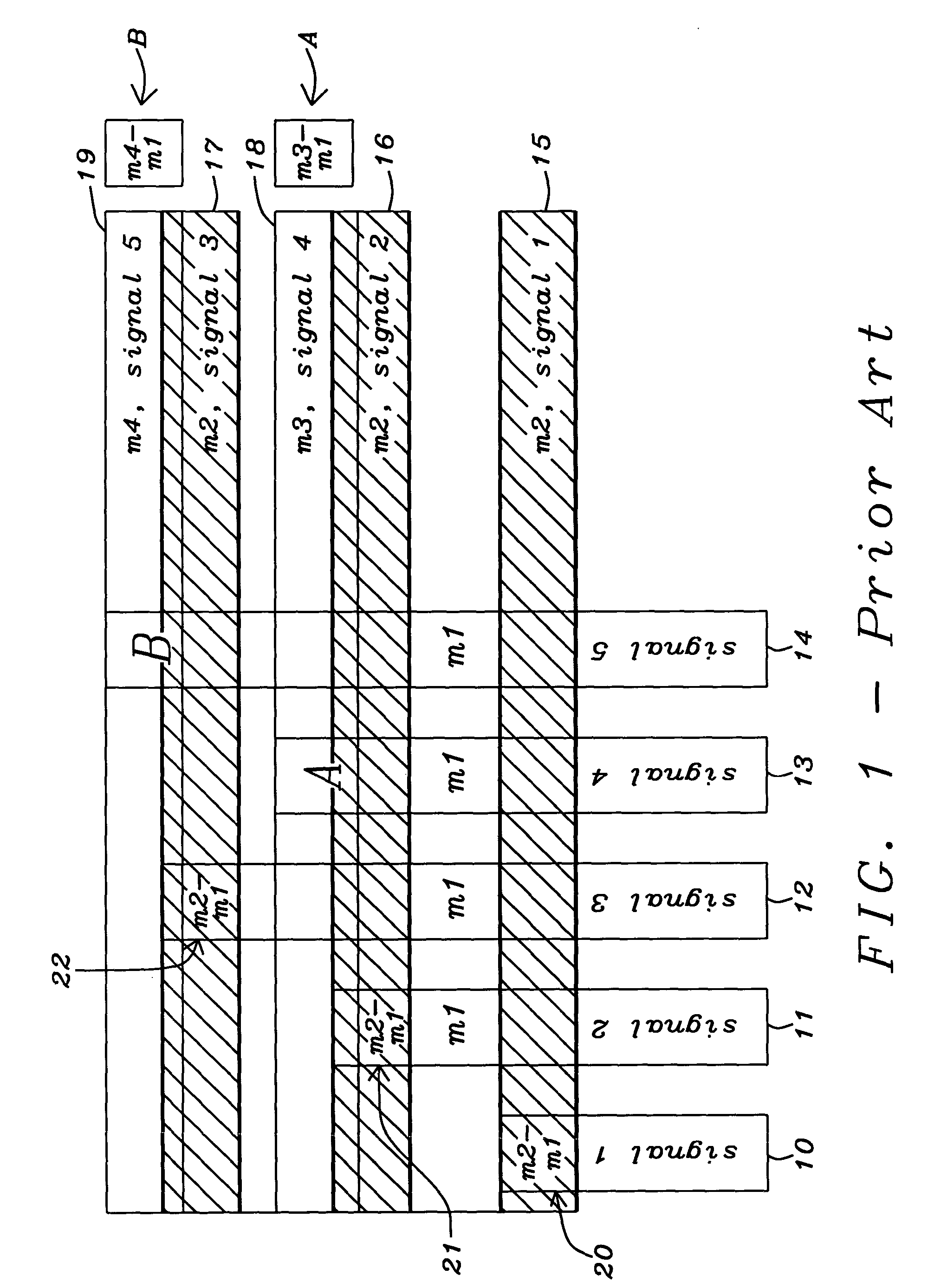
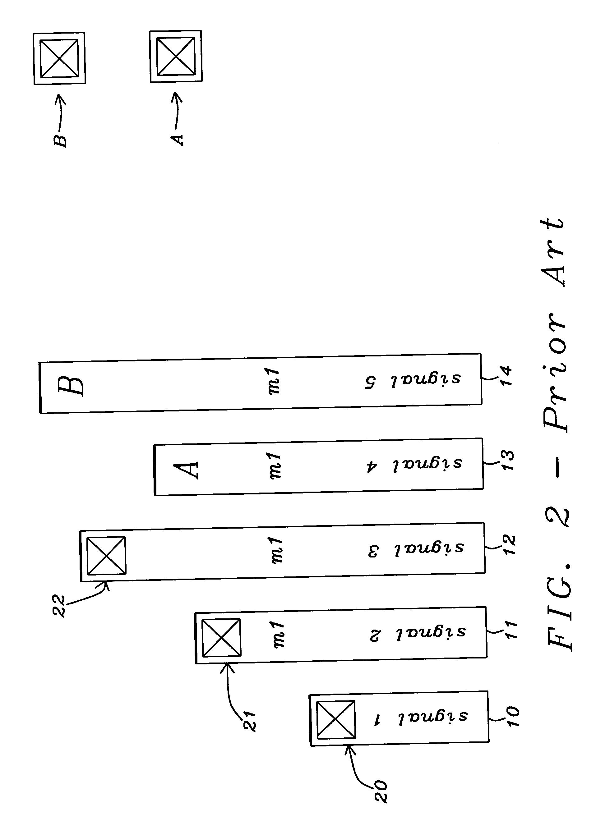
[0031] The ground rules that are provided by the invention are stated first, examples of the ground rules will be shown using FIGS. 1 through 6 for that purpose.

[0032] Before the prior art methods are explained, it is of value to first highlight the method and structure on which the invention is based. The invention provides for: [0033] reserving a channel for the creation of via interconnects vertically overlying the channel [0034] creating no vias on parallel interconnect traces of the interconnect network [0035] stacking the interconnect traces [0036] providing parallel interconnect traces [0037] creating multiple overlying layers of metal by repeating a basic pattern of interconnect and there-with associated vias, and [0038] placing the vias over the therefore reserved channel and providing interconnects between the vias and the interconnect traces.

[0039] Prior Art methods of creating interconnect metal and the there-with experienced problems will now be explained using FIGS. ...


PUM


Abstract

In accordance with the objectives of the invention a new method and structure is provided for the creation of multiple overlying layers of interconnect metal. A channel is reserved for the creation of via interconnects, no vias are placed on metal lines. The metal lines are stacked and parallel, whereby a space is provided between lines that is reserved for the creation of vias for layer interconnection. This structure can be repeated, the vias are placed on the therefore reserved channel, interconnections are provided to the interconnect traces.

Description

BACKGROUND OF THE INVENTION [0001] (1) Field of the Invention [0002] The invention relates to the fabrication of integrated circuit devices, and more particularly, to a method of routing multiple layers of metal. [0003] (2) Description of the Prior Art [0004] Ever increasingly complex and densely packaged semiconductor devices require extensive networks of interconnect metal, a requirement that is especially demanding in the design of standard cell and gate array containing devices in view of the repetitive nature of these structures. [0005] The demands of creating interconnect metal is further driven by demands of creating designs such as gate arrays in basic patterns after which multiple of these patterns can be interconnected to create interconnections that are specifically customer dependent and by thereby creating specialized and unique customer designs. This provides a cost-effective method of creating high-density, high-performance customized devices that perform logic functi...

Claims


Application Information

Patent Timeline
Patent Type & Authority Applications(United States)
IPC IPC(8): H01L23/528
CPCH01L23/528H01L2924/0002H01L2924/00
Inventor JAN, TZONG-SHI
Owner TAIWAN SEMICON MFG CO LTD
Learn More