Method of defect root cause analysis
a root cause analysis and defect technology, applied in the field of can solve the problems of root cause analysis also having a serious blind spot, small particles and defects are unavoidable, and affect the property of the integrated circuit more seriously, so as to improve the sensitivity reduce the judging time of the defect root cause analysis, and improve the yield and reliability of products
- Summary
- Abstract
- Description
- Claims
- Application Information
AI Technical Summary
Benefits of technology
Problems solved by technology
Method used
Image
Examples
first embodiment
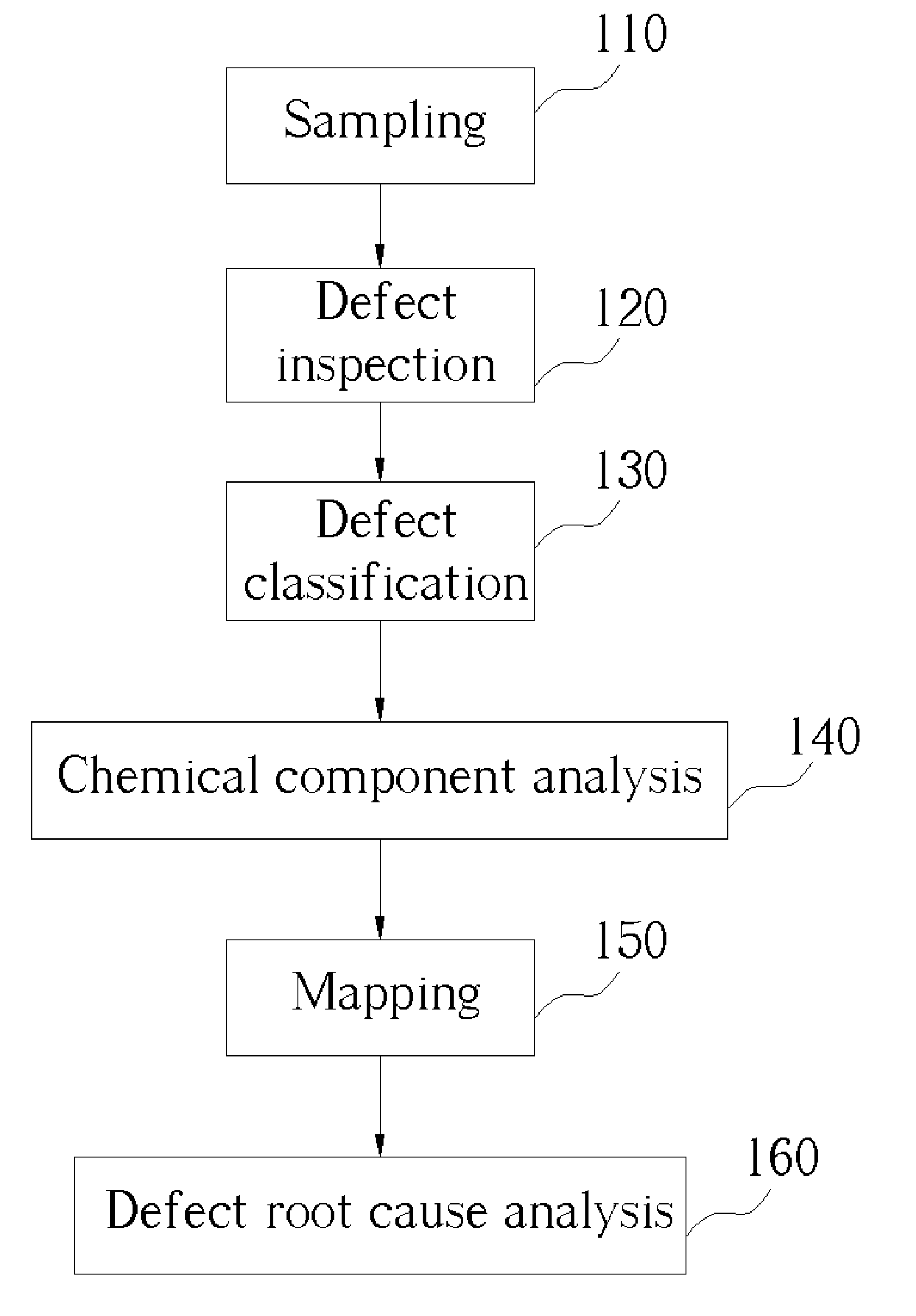
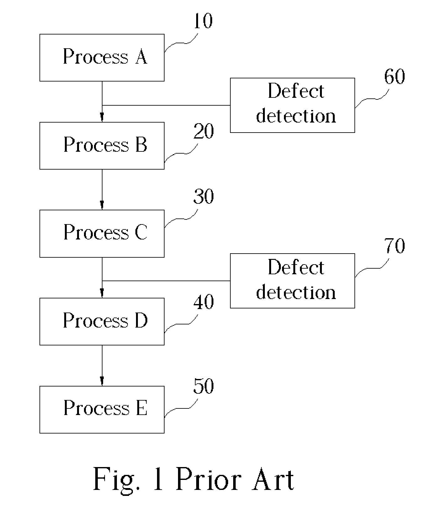
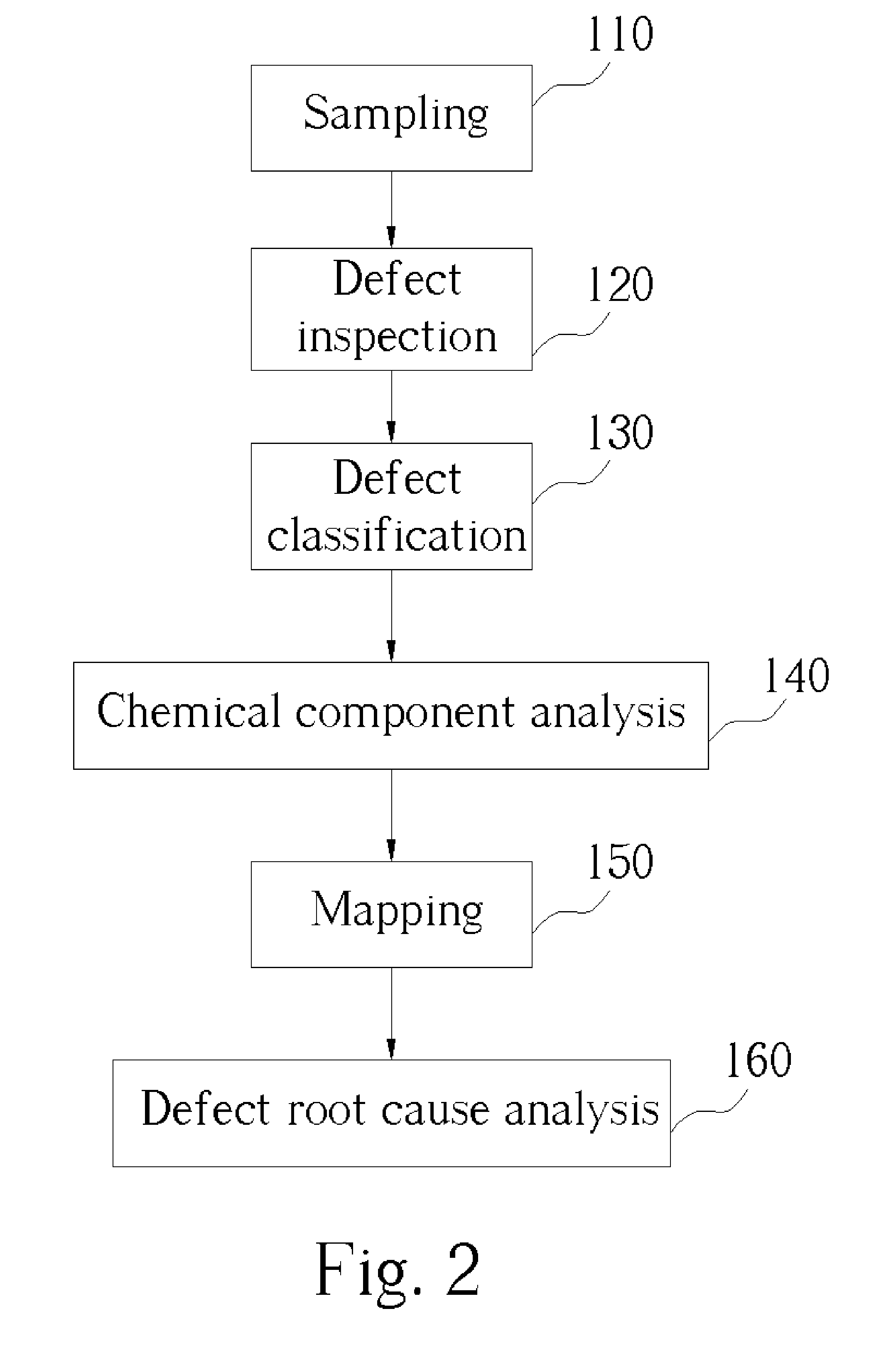
[0025] To describe the method of the present invention in detail, two embodiments are provided in following. An analysis according to the conventional method is also provided as a contrast to show the differences between the method of the present invention and that in the prior art. First, a common etching process is illustrated in the present invention to describe the method of defect root cause analysis in the present invention. For example, it is supposed that we want to form a patterned tungsten (W) conductive line on a silicon oxide layer, but the W conductive line shorts, which is treated as a defect, after the etching process. By using the conventional method of defect root cause analysis, a short loop inspection plan must be set up to trace 3 to 5 processes before the process in which defects are detected and a step by step check is performed to find out the exact process in which the defects occurs. For example, if the defects are only found after the etching process, it is...
second embodiment
[0027] Next, a deposition process is illustrated for describing a case which has defects located in the underlayer of the test sample. Please refer to FIG. 5, which is a schematic diagram of the method of defect root cause analysis according to the present invention. Taking a TiN deposition process as an example, it is supposed that some defects are found in the underlayer of a test sample during the defect inspection 320. According to the conventional method, it will trace the previous process step by step and find the defects are generated in the deposition process. The EDS analysis will only show that the defects are formed by Ti and N, which are similar to those in the background. Thus, no conclusion can be made. As shown in FIG. 5, according to the method of the present invention, if the defects are found by the SEM in the defect inspection 320, the FIB analysis 330 is performed to cut the test sample. Then, an auger analysis 340 is performed in the same manner to analyze the c...
PUM
 Abstract
Description
Claims
Application Information
 - R&D
- Intellectual Property
- Life Sciences
- Materials
- Tech Scout
- Unparalleled Data Quality
- Higher Quality Content
- 60% Fewer Hallucinations
Browse by: Latest US Patents, China's latest patents, Technical Efficacy Thesaurus, Application Domain, Technology Topic, Popular Technical Reports.
© 2025 PatSnap. All rights reserved.Legal|Privacy policy|Modern Slavery Act Transparency Statement|Sitemap|About US| Contact US: help@patsnap.com


