Gettering using voids formed by surface transformation

a surface transformation and void technology, applied in semiconductor devices, semiconductor/solid-state device details, electrical devices, etc., can solve the problems of small thermal budget of modem low-temperature processes, inability to afford significant diffusion of dopants, and undesirable effects, etc., to achieve the effect of increasing the surface to volume ratio and increasing the gettering of impurities

Inactive Publication Date: 2005-02-10
MICRON TECH INC
View PDF99 Cites 53 Cited by
  • Summary
  • Abstract
  • Description
  • Claims
  • Application Information

AI Technical Summary

Problems solved by technology

These defect and impurities can degrade device characteristics and overall yield.
However, modem low temperature processes have small thermal budgets, and do not afford an opportunity for significant diffusion of dopants and / or unwanted impurities.
One problem associated with the random location and density of cavities is that the effectiveness of the gettering unwanted impurities from the desired device regions is inconsistent.
Other problems associated with the random location and density of cavities involves the varying strain in the substrate and the varying ability of the substrate to withstand mechanical strain.
The inconsistent effectiveness of gettering, the inconsistent strain and the inconsistent ability to withstand strain can negatively affect the ability to precisely form devices as the semiconductor industry strives to fabricate smaller and thinner devices.

Method used


Image

  • Gettering using voids formed by surface transformation
  • Gettering using voids formed by surface transformation
  • Gettering using voids formed by surface transformation

Examples


Embodiment Construction

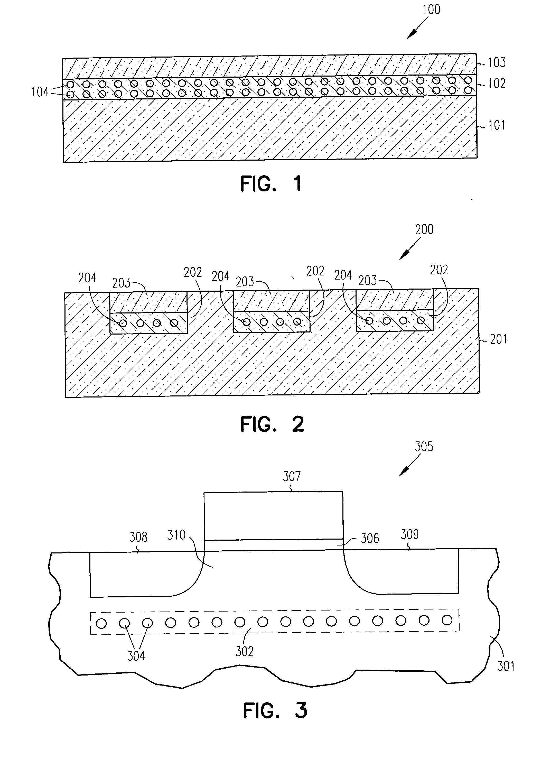
The following detailed description refers to the accompanying drawings which show, by way of illustration, specific aspects and embodiments in which the present invention may be practiced. The various embodiments are not necessarily mutually exclusive as aspects of one embodiment can be combined with aspects of another embodiment. Other embodiments may be utilized and structural, logical, and electrical changes may be made without departing from the scope of the present invention. In the following description, the terms wafer and substrate are interchangeably used to refer generally to any structure on which integrated circuits are formed, and also to such structures during various stages of integrated circuit fabrication. Both terms include doped and undoped semiconductors, epitaxial layers of a semiconductor on a supporting semiconductor or insulating material, combinations of such layers, as well as other such structures that are known in the art. The terms “horizontal” and “ver...


PUM


Abstract

One aspect of this disclosure relates to a method for creating a gettering site in a semiconductor wafer. In various embodiments, a predetermined arrangement of a plurality of holes is formed in the semiconductor wafer through a surface of the wafer. The wafer is annealed such that the wafer undergoes a surface transformation to transform the arrangement of the plurality of holes into a predetermined arrangement of at least one empty space of a predetermined size within the wafer to form the gettering site. One aspect relates to a semiconductor wafer. In various embodiments, the wafer includes at least one device region, and at least one gettering region located proximate to the at least one device region. The gettering region includes a precisely-determined arrangement of a plurality of precisely-formed voids that are formed within the wafer using a surface transformation process. Other aspects and embodiments are provided herein.

Description

TECHNICAL FIELD This disclosure relates generally to integrated circuits, and more particularly, to strained semiconductor structures. BACKGROUND Unwanted crystalline defects and impurities can be introduced during crystal growth or subsequent wafer fabrication processes. These defect and impurities can degrade device characteristics and overall yield. Gettering has been described as a process for moving contaminants and / or defects in a semiconductor into its bulk and away from its top surface to create a denuded zone cleared from contaminants and / or defects. Preferably, devices are built in the denuded zone. Historically, extrinsic backside gettering was used to getter silicon wafers. Various extrinsic backside gettering processes involve damaging the backside of the wafer mechanically or by implanting argon, germanium, hydrogen or other implants, or providing a gettering layer on the backside of the wafer using a phophorosilicate glass or oxide backside layer, a polysilicon bac...

Claims


Application Information

Patent Timeline
Patent Type & Authority Applications(United States)
IPC IPC(8): H01L21/322H01L21/324H01L29/78
CPCH01L21/3223H01L21/324H01L29/78H01L27/108H01L27/105Y10S257/913H10B12/00
Inventor FORBES, LEONARDGEUSIC, JOSEPH E.
Owner MICRON TECH INC
Why Eureka
Try Eureka